• HOME
  • NEWS
  • EXPLORE
    • CAREER
      • Companies
      • Jobs
    • EVENTS
    • iGEM
      • News
      • Team
    • PHOTOS
    • VIDEO
    • WIKI
  • BLOG
  • COMMUNITY
    • FACEBOOK
    • INSTAGRAM
    • TWITTER
Friday, May 15, 2026
BIOENGINEER.ORG
No Result
View All Result
  • Login
  • HOME
  • NEWS
  • EXPLORE
    • CAREER
      • Companies
      • Jobs
        • Lecturer
        • PhD Studentship
        • Postdoc
        • Research Assistant
    • EVENTS
    • iGEM
      • News
      • Team
    • PHOTOS
    • VIDEO
    • WIKI
  • BLOG
  • COMMUNITY
    • FACEBOOK
    • INSTAGRAM
    • TWITTER
No Result
View All Result
Bioengineer.org
No Result
View All Result
Home NEWS Science News Chemistry

Organic electronics: a new semiconductor in the carbon-nitride family

Bioengineer by Bioengineer
June 6, 2019
in Chemistry
Reading Time: 3 mins read
0
IMAGE
Share on FacebookShare on TwitterShare on LinkedinShare on RedditShare on Telegram

IMAGE

Credit: C. Merschjann/HZB

Some organic materials might be able to be utilised similarly to silicon semiconductors in optoelectronics. Whether in solar cells, light-emitting diodes, or in transistors – what is important is the band gap, i.e. the difference in energy level between electrons in the valence band (bound state) and the conduction band (mobile state). Charge carriers can be raised from the valence band into the conduction band by means of light or an electrical voltage. This is the principle behind how all electronic components operate. Band gaps of one to two electron volts are ideal.

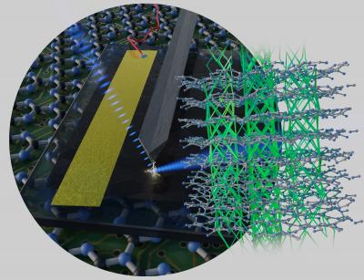
A team headed by chemist Dr. Michael J. Bojdys at Humboldt University Berlin recently synthesised a new organic semiconductor material in the carbon-nitride family. Triazine-based graphitic carbon nitride (or TGCN) consists of only carbon and nitrogen atoms, and can be grown as a brown film on a quartz substrate.The combination of C and N atoms form hexagonal honeycombs similar to graphene, which consists of pure carbon.Just as with graphene, the crystalline structure of TGCN is two-dimensional.With graphene, however, the planar conductivity is excellent, while its perpendicular conductivity is very poor. In TGCN it is exactly the opposite: the perpendicular conductivity is about 65 times greater than the planar conductivity. With a band gap of 1.7 electron volts, TGCN is a good candidate for applications in optoelectronics.

HZB physicist Dr. Christoph Merschjann subsequently investigated the charge transport properties in TGCN samples using time-resolved absorption measurements in the femto- to nanosecond range at the JULiq laser laboratory, a JointLab between HZB and Freie Universität Berlin. These kinds of laser experiments make it possible to connect macroscopic electrical conductivity with theoretical models and simulations of microscopic charge transport. From this approach he was able to deduce how the charge carriers travel through the material. “They do not exit the hexagonal honeycombs of triazine horizontally, but instead move diagonally to the next hexagon of triazine in the neighbouring plane. They move along tubular channels through the crystal structure.” This mechanism might explain why the electrical conductivity perpendicular to the planes is considerably higher than that along the planes. However, this is probably not sufficient to explain the actual measured factor of 65. “We do not yet fully understand the charge transport properties in this material and want to investigate them further”, adds Merschjann. At ULLAS / HZB in Wannsee, the analysis lab used subsequent to JULiq, the setup is being prepared for new experiments to accomplish this.

“TGCN is therefore the best candidate so far for replacing common inorganic semiconductors like silicon and their crucial dopants, some of which are rare elements”, says Bojdys. “The fabrication process we developed in my group at Humboldt-Universität, produces flat layers of semiconducting TGCN on an insulating quartz substrate. This facilitates upscaling and simple fabrication of electronic devices.”

###

Media Contact
Antonia Roetger
[email protected]

Original Source

https://www.helmholtz-berlin.de/pubbin/news_seite?nid=20603;sprache=en;seitenid=1

Related Journal Article

http://dx.doi.org/10.1002/anie.201902314

Tags: Chemistry/Physics/Materials SciencesIndustrial Engineering/ChemistryMaterials
Share12Tweet8Share2ShareShareShare2

Related Posts

Synthetic Cell Microreactor with Dual Dynamic DNA Pores — Chemistry

Synthetic Cell Microreactor with Dual Dynamic DNA Pores

May 15, 2026
Hanyang University Researchers Pinpoint 2.5 Nanometers as Minimum Coating Thickness for Durable Solid-State EV Batteries — Chemistry

Hanyang University Researchers Pinpoint 2.5 Nanometers as Minimum Coating Thickness for Durable Solid-State EV Batteries

May 15, 2026

Smart Hydrogels Revolutionize Information Security with Photo-Patterning and Multi-Stimuli Responsive Structural Colors

May 15, 2026

Scientists Overcome Longstanding Challenge in Measuring Semiconductor Defects

May 14, 2026
Please login to join discussion

POPULAR NEWS

  • Research Indicates Potential Connection Between Prenatal Medication Exposure and Elevated Autism Risk

    843 shares
    Share 337 Tweet 211
  • New Study Reveals Plants Can Detect the Sound of Rain

    729 shares
    Share 291 Tweet 182
  • Salmonella Haem Blocks Macrophages, Boosts Infection

    62 shares
    Share 25 Tweet 16
  • Breastmilk Balances E. coli and Beneficial Bacteria in Infant Gut Microbiomes

    58 shares
    Share 23 Tweet 15

About

We bring you the latest biotechnology news from best research centers and universities around the world. Check our website.

Follow us

Recent News

Autism Subtypes Revealed Through Cross-Species Brain Mapping

Synthetic Cell Microreactor with Dual Dynamic DNA Pores

Key Drivers of Energy Policy Support in Europe

Subscribe to Blog via Email

Enter your email address to subscribe to this blog and receive notifications of new posts by email.

Join 82 other subscribers
  • Contact Us

Bioengineer.org © Copyright 2023 All Rights Reserved.

Welcome Back!

Login to your account below

Forgotten Password?

Retrieve your password

Please enter your username or email address to reset your password.

Log In
No Result
View All Result
  • Homepages
    • Home Page 1
    • Home Page 2
  • News
  • National
  • Business
  • Health
  • Lifestyle
  • Science

Bioengineer.org © Copyright 2023 All Rights Reserved.