High-throughput double anodization to make ordered titania through-hole membranes
Credit: Tokyo Metropolitan University
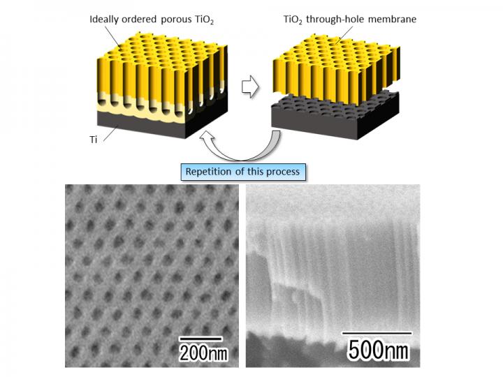
Tokyo, Japan – Researchers from Tokyo Metropolitan University have realized high-throughput production of thin, ordered through-hole membranes of titanium dioxide. Titania layers were grown using anodization on mask-etched titanium before being crystallized. Applying a second anodization, they converted part of the layer back to an amorphous state. The amorphous portion was then selectively dissolved to free the film while leaving the template intact. This paves the way for industrial production of ordered titania membranes for photonics.
Titania, or titanium dioxide, might be the most useful substance you’ve never heard of. It is widely used as a pigment, and is the active ingredient in most sunscreens, with strong UV absorbing properties. It is found as a reflective layer in mirrors, as well as coatings for self-cleaning, anti-fogging surfaces. Importantly for industry, it can accelerate all sorts of chemical reactions in the presence of light; it is already found in building materials to speed up the breakdown of harmful pollutants in the air, with work under way to apply it to air filters, water purifiers and solar cells.
It’s the strong interaction between titania and light that makes it the future material for a wide range of applications involving photonics, particularly photonic crystals, ordered arrays of material which can absorb or transmit light depending on their wavelength. To make these “crystals,” researchers have come up with ways of creating porous titania films in the lab, where tiny holes, tens of nanometers across, are patterned onto thin titanium dioxide layers in ordered arrays. Despite their promise, however, it is still not possible to produce them at scale, a major stumbling block for getting them out of the lab and into the latest photonic tech.
Now, a team led by Associate Professor Takashi Yanagishita and Prof. Hideki Masuda of Tokyo Metropolitan University have taken an important step towards developing an industrial production process. Previously, they came up with a method of “stamping” patterns on titanium metal before growing a layer of titanium dioxide using a method called anodization. The layers had holes which formed the same pattern as the ones made artificially on the metal. But because titanium is so hard, the stamps didn’t last very long. Now, they’ve come up with a method that avoids stamps altogether. After they grow a layer of titania with ordered arrays of holes on an etched titanium template, they apply heat, changing the amorphous, disordered structure of the titania into a crystalline form. They then go through a second anodization; a layer close to the original template surface returns to a disordered state. Because disordered and crystalline titania dissolve differently, they are then able to selectively dissolve away the layer still in contact with the template using acid, leaving a free layer of titania with the same through hole pattern.
Of the many advantages of their method, a key benefit is that the template pattern on the metal is left intact. After the film is removed, the same template can be reused over and over again. The team also experimented with different spacings, going down to holes spaced by a mere 100nm. Importantly, the protocol is scalable and high-throughput, meaning that it might not be long before industrial quantities make their way into commercial products. The team hopes their method will not only bring widespread application a step closer, but be applied to a wide range of other nanostructured materials with different functions.
###
This work was supported by the Light Metal Educational Foundation and a JSPS KAKENHI Grant (20K05171).
Media Contact
Go Totsukawa
[email protected]
Original Source
https:/
Related Journal Article
http://dx.
