
In a landmark advancement poised to revolutionize data storage technology, researchers at the Max Born Institute have unveiled a pioneering method to manipulate magnetic bits at the nanoscale with exceptional speed and precision using ultrafast laser pulses coupled with plasmonic gold nanostructures. The breakthrough centers on the harnessing of all-optical, helicity-independent magnetization switching (AO-HIS), a process that enables the direct reversal of magnetization states using single femtosecond light pulses without the need for external magnetic fields or complex circuitry. This achievement promises a new generation of memory devices that are not only ultrafast and energy-efficient but capable of unprecedented miniaturization, transcending current technological limitations.
Magnetization switching is fundamental to digital data encoding, wherein binary “0s” and “1s” correspond to distinct magnetic orientations. Traditional methods rely on magnetic fields or electrical currents, which impose speed constraints and consume significant power. The AO-HIS mechanism, however, bypasses such constraints by employing sub-picosecond laser pulses that toggle magnetic states directly and deterministically. More intriguingly, the helicity independence means that the polarization of the laser light does not influence switching, greatly simplifying device design and reliability.
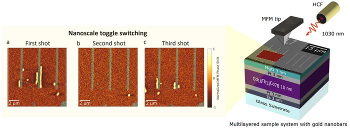
This study delves into nanoscale magnetization control where the challenge lies in pushing the physical boundaries of bit size without compromising stability or switching fidelity. The researchers tackled this by integrating plasmonic gold nanostructures fabricated with electron beam lithography atop a specialized thin magnetic film formed from a Rare Earth – Transition Metal (RE-TM) alloy known as GdTbCo. The presence of terbium, a rare earth element, endows the magnetic layer with pronounced anisotropy conducive to stabilizing exceedingly small magnetic domains essential for dense data storage architectures.
At the heart of the technique is the use of a 370 femtosecond laser pulse at a wavelength of 1030 nm. The gold nanobars serve as plasmonic antennas, localizing and enhancing the electromagnetic field at the nanoscale well beyond the natural diffraction limit of light. This enhanced confinement not only reduces the laser energy required for magnetization switching but also defines the spatial extent of the switched magnetic domain, achieving magnetic reversal within mere 240-nanometer regions. Such spatial control is critical for designing memory cells at dimensions that rival or exceed contemporary semiconductor technologies.
Exceptional control over magnetization was demonstrated through a series of targeted laser pulses. Initially, a single pulse focused on the plasmonic nanobars induced a localized reversal of magnetic orientation precisely along the nanobar edges. Thereafter, a subsequent laser pulse of identical fluence toggled the reversed state back to its original magnetic orientation, affirming the reversible and deterministic nature of the switching process. This toggling capability mirrors the essential binary operation in computing, confirming that these nanoscale magnetization states can effectively encode information.
The use of magnetic force microscopy (MFM) was integral to visualizing these magnetic states with nanometric precision. This high-resolution scanning probe technique was employed in situ, enabling direct observation of magnetic domain configurations immediately after each laser-induced switching event. The resulting images provide indispensable insight into the spatial dynamics and stability of the magnetization states, pillars for advancing ultrafast magnetic memory technologies.
Beyond toggle switching, the researchers observed complex magnetization patterns under varying plasmonic resonance conditions. When the excitation laser was off-resonance with the plasmonic nanostructures, the magnetic film displayed a dipole-like far-field scattering domain pattern, effectively “imprinted” onto the magnetic material. This phenomenon opens avenues to probe how different plasmonic energy transfer mechanisms underpin magnetic domain formation and manipulation at the nanoscale, revealing fundamental physics while guiding future device optimization.
The experimental approach sheds light on critical open questions surrounding nanoscale heat transfer and magnetic domain wall propagation, which traditionally impose theoretical and practical limits on the minimal stable bit size achievable. By controlling plasmon excitation both on- and off-resonance, nuanced insights into heat and spin dynamics were gained, challenges integral to designing next-generation ultrafast memory chips.
This research propagates a transformative vision for spintronic and opto-magnetic technologies. Compact, fast, and energy-frugal magnetic memories could replace or complement existing volatile and non-volatile memory solutions, driving down latency, boosting data throughput, and enabling on-chip memory architectures that leverage light–magnetism interactions. Such systems would reshape computational paradigms, particularly for high-performance and quantum information technologies that seek tight integration of data storage with light-based processing.
Puloma Singh, a key researcher driving this project as part of her doctoral studies at the Max Born Institute, emphasizes the fundamental nature of this work while envisioning its expansive technological impact. The foundational understanding gained from localized optical switching experiments will inform the future engineering of magnetic materials and excitation strategies, ultimately enabling light-controlled magnetism to reach its full potential in nanoscale devices.
The implications of this study reach far beyond basic magnetic switching. By bridging plasmonics with magneto-optical control, the work pioneers innovative methodologies to surpass conventional physical limits of data storage densities. Ultrafast laser pulses become not mere tools but enablers of precise, reversible, and energy-efficient magnetic state control, poised to catalyze the evolution of digital technologies.
The detailed experimental setup, leveraging ultrashort laser pulses, delicate lithographic fabrication of plasmonic nanostructures, and sensitive magnetic force microscopy characterization, is testimony to the interdisciplinary nature of modern condensed matter and optical physics research. Such convergence of expertise drives breakthroughs essential to meet the insatiable global demand for faster, smaller, and greener data storage solutions.
This work, published in the prestigious journal Nano Letters, marks a significant milestone in materials science and magneto-optical technology, promising to energize subsequent studies exploring ultrafast light-matter interactions at unrivaled spatial and temporal scales. As the relentless push toward miniaturization continues, these subwavelength localized switching mechanisms spotlight an innovative pathway to redefine the limits of memory device engineering.
—
Subject of Research: Not applicable
Article Title: Subwavelength Localized All-Optical Helicity-Independent Magnetic Switching Using Plasmonic Gold Nanostructures
News Publication Date: 18-Mar-2025
Web References: http://dx.doi.org/10.1021/acs.nanolett.4c04024
Image Credits: MBI: T.P.H. Sidiropoulos, P. Singh
Keywords
All-optical magnetization switching, helicity-independent switching, plasmonics, gold nanostructures, ultrafast laser pulses, nanoscale data storage, magnetic force microscopy, spintronics, rare earth-transition metal alloys, GdTbCo, femtosecond laser, nanomagnetic domains
Tags: all-optical magnetization switchingdata storage advancementsdigital data encoding techniquesenergy-efficient memory deviceshelicity-independent magnetization controlminiaturization in electronicsnanoscale magnetic bit switchingoptical manipulation of magnetizationovercoming traditional magnetic switching limitationsplasmonic gold nanostructuressub-picosecond laser technologyultrafast laser pulses


