Researchers make graphene tunable, opening up its band gap to a record 2.1 electronvolts
Credit: Purdue University image/Gary Cheng
WEST LAFAYETTE, Ind. — In 2004, researchers discovered a super thin material that is at least a 100 times stronger than steel and the best known conductor of heat and electricity.
This means that the material, graphene, could bring faster electronics than is possible today with silicon.
But to truly be useful, graphene would need to carry an electric current that switches on and off, like what silicon does in the form of billions of transistors on a computer chip. This switching creates strings of 0s and 1s that a computer uses for processing information.
Purdue University researchers, in collaboration with the University of Michigan and the Huazhong University of Science and Technology, show how a laser technique could permanently stress graphene into having a structure that allows the flow of electric current.
This structure is a so-called “band gap.” Electrons need to jump across this gap in order to become conduction electrons, which makes them capable of carrying electric current. But graphene doesn’t naturally have a band gap.
Purdue researchers created and widened the band gap in graphene to a record 2.1 electronvolts. To function as a semiconductor such as silicon, the band gap would need to be at least the previous record of 0.5 electronvolts.
“This is the first time that an effort has achieved such high band gaps without affecting graphene itself, such as through chemical doping. We have purely strained the material,” said Gary Cheng, professor of industrial engineering at Purdue, whose lab has investigated various ways to make graphene more useful for commercial applications.
The presence of a band gap allows semiconductor materials to switch between insulating or conducting an electric current, depending on whether their electrons are pushed across the band gap or not.
Surpassing 0.5 electronvolts unlocks even more potential for graphene in next-generation electronic devices, the researchers say. Their work appears in an issue of Advanced Materials.
“Researchers in the past opened the band gap by simply stretching graphene, but stretching alone doesn’t widen the band gap very much. You need to permanently change the shape of graphene to keep the band gap open,” Cheng said.
Cheng and his collaborators not only kept the band gap open in graphene, but also made it to where the gap width could be tuned from zero to 2.1 electronvolts, giving scientists and manufacturers the option to just use certain properties of graphene depending on what they want the material to do.
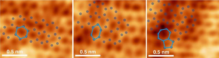
The researchers made the band gap structure permanent in graphene using a technique called laser shock imprinting, which Cheng developed in 2014 along with scientists at Harvard University, the Madrid Institute for Advanced Studies and the University of California, San Diego.
For this study, the researchers used a laser to create shockwave impulses that penetrated an underlying sheet of graphene. The laser shock strains graphene onto a trench-like mold – permanently shaping it. Adjusting the laser power adjusts the band gap.
While still far from putting graphene into semiconducting devices, the technique grants more flexibility in taking advantage of the material’s optical, magnetic and thermal properties, Cheng said.
###
The work was supported by multiple entities, including the National Science Foundation (Grant numbers CMMI-0547636 and CMMI 0928752) and the National Research Council Senior Research Associateship.
ABSTRACT
Asymmetric 3D Elastic-Plastic Strain-Modulated Electron Energy Structure in Monolayer Graphene by Laser Shocking
Maithilee Motlag1, Prashant Kumar1, Kevin Y. Hu1, Shengyu Jin1, Ji Li1, Jiayi Shao1, Xuan Yi1, Yen-Hsiang Lin2, Jenna C. Walrath2, Lei Tong3, Xinyu Huang3, Rachel S. Goldman2, Lei Ye3, and Gary J. Cheng1
1Purdue University, West Lafayette, IN, USA
2University of Michigan, Ann Arbor, MI, USA
3Huazhong University of Science and Technology, Wuhan, China
doi: 10.1002/adma.201900597
Graphene has a great potential to replace silicon in prospective semiconductor industries due to its outstanding electronic and transport properties; nonetheless, its lack of energy bandgap is a substantial limitation for practical applications. To date, straining graphene to break its lattice symmetry is perhaps the most efficient approach toward realizing bandgap tunability in graphene. However, due to the weak lattice deformation induced by uniaxial or in?plane shear strain, most strained graphene studies have yielded bandgaps
Media Contact
Kayla Wiles
[email protected]
Original Source
https:/
Related Journal Article
http://dx.

