• HOME
  • NEWS
  • EXPLORE
    • CAREER
      • Companies
      • Jobs
    • EVENTS
    • iGEM
      • News
      • Team
    • PHOTOS
    • VIDEO
    • WIKI
  • BLOG
  • COMMUNITY
    • FACEBOOK
    • INSTAGRAM
    • TWITTER
Monday, August 18, 2025
BIOENGINEER.ORG
No Result
View All Result
  • Login
  • HOME
  • NEWS
  • EXPLORE
    • CAREER
      • Companies
      • Jobs
        • Lecturer
        • PhD Studentship
        • Postdoc
        • Research Assistant
    • EVENTS
    • iGEM
      • News
      • Team
    • PHOTOS
    • VIDEO
    • WIKI
  • BLOG
  • COMMUNITY
    • FACEBOOK
    • INSTAGRAM
    • TWITTER
No Result
View All Result
Bioengineer.org
No Result
View All Result
Home NEWS Science News Chemistry

Pumping perovskites into a semiconductor platform

Bioengineer by Bioengineer
March 1, 2021
in Chemistry
Reading Time: 2 mins read
0
Share on FacebookShare on TwitterShare on LinkedinShare on RedditShare on Telegram

IMAGE

Credit: © 2021 KAUST; Heno Hwang

Materials called perovskites can be more readily incorporated into silicon-based semiconducting platforms by using a microfluidic pumping technology developed at KAUST.

The perovskites currently being explored for many applications in new technologies are diverse materials sharing the same crystalline structure as the natural mineral perovskite. These semiconducting materials show great promise in a variety of optoelectronic applications, such as light emitters, sensors and solar cells.

Compared to traditional semiconductors, perovskites are soft and unstable. “This makes it difficult to pattern them using standard lithography methods,” says materials scientist Iman Roqan at KAUST.

The challenge tackled by Roqan and her colleagues was to adapt microfluidic technologies to manipulate solutions carrying perovskites to create semiconducting microscale wires.

The first step in the procedure is to create the desired pattern of microchannels in a silicon wafer using a laser interference technique. The key innovation is to pump a solution containing perovskite ions into these microchannels, where the perovskite solidifies into the network of semiconductor wires.

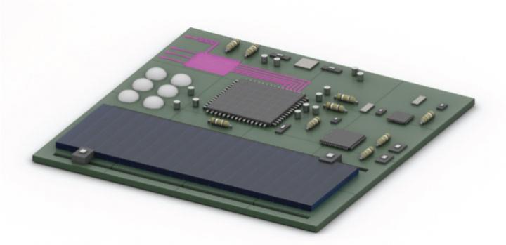
“We are the first researchers to achieve this,” says Roqan, adding that the innovation, which has now been patented, will allow several different perovskite-based optoelectronic devices to be located on one silicon chip. For example, a single chip could embody a photodetector, transistor, light-emitting diode and a solar cell to act as the power supply.

To demonstrate the potential of the technique, the team have built a high-performance photodetector.

“Unlike other options, our fabrication method is extremely simple and cost-effective, while avoiding creating waste materials,” Roqan says. Some metals used in perovskites are toxic, so avoiding their release into the environment is a significant advantage.

There remain challenges to overcome to advance from this initial proof-of-concept stage. For example, the team is working to bring the stability of the devices up to a standard suitable for large-scale industrial applications. Roqan expects that work currently in progress to achieve this is likely to lead to further patents, while also building more complex demonstration devices.

One of the most likely areas for commercial development is in the growing field of “lab on a chip” technology. This can combine processes such as sensing, signaling, microfluid manipulation and chemical separations and combinations to miniaturize many laboratory procedures used in medicine and biology. With miniaturization comes portability, potentially taking a full testing laboratory process out of the lab and into the outside world.

###

Media Contact
Michael Cusack
[email protected]

Original Source

https://discovery.kaust.edu.sa/en/article/1100/pumping-perovskites-into-a-semiconductor-platform

Related Journal Article

http://dx.doi.org/10.1016/j.xcrp.2020.100304

Tags: Chemistry/Physics/Materials SciencesIndustrial Engineering/ChemistryMaterialsNanotechnology/MicromachinesSuperconductors/Semiconductors
Share12Tweet8Share2ShareShareShare2

Related Posts

blank

Reusable ‘jelly ice’ stays cold without melting into water

August 18, 2025
A Laser-Free Alternative to LASIK: Exploring New Vision Correction Methods

A Laser-Free Alternative to LASIK: Exploring New Vision Correction Methods

August 18, 2025

Fe-Lattice O–O Ligands Boost Water Oxidation Catalysis

August 18, 2025

Innovative Technology Developed to Precisely Control Pore Wall Crystallinity

August 18, 2025
Please login to join discussion

POPULAR NEWS

  • blank

    Molecules in Focus: Capturing the Timeless Dance of Particles

    141 shares
    Share 56 Tweet 35
  • Neuropsychiatric Risks Linked to COVID-19 Revealed

    80 shares
    Share 32 Tweet 20
  • Modified DASH Diet Reduces Blood Sugar Levels in Adults with Type 2 Diabetes, Clinical Trial Finds

    59 shares
    Share 24 Tweet 15
  • Predicting Colorectal Cancer Using Lifestyle Factors

    47 shares
    Share 19 Tweet 12

About

We bring you the latest biotechnology news from best research centers and universities around the world. Check our website.

Follow us

Recent News

Ensuring Precision in SABR-ROC Trial Quality

eIF2B Activator DNL343 Targets ALS and TDP-43

Comparing Bioactive Compounds in Justicia spicigera Extracts

  • Contact Us

Bioengineer.org © Copyright 2023 All Rights Reserved.

Welcome Back!

Login to your account below

Forgotten Password?

Retrieve your password

Please enter your username or email address to reset your password.

Log In
No Result
View All Result
  • Homepages
    • Home Page 1
    • Home Page 2
  • News
  • National
  • Business
  • Health
  • Lifestyle
  • Science

Bioengineer.org © Copyright 2023 All Rights Reserved.