Credit: by David Knez, Adam Hanninen, Richard Prince, Eric Potma and Dmitry Fishman
The MIR range of the electromagnetic spectrum, which roughly covers light in the wavelength regime between 3 to 10 micrometers, coincides with the energies of fundamental molecular vibrations. Utilizing this light for the purpose of imaging can produce stills with chemical specificity, i.e. images with contrast derived from the chemical composition of the sample. Unfortunately, detecting MIR light is not as simple as detecting light in the visible regime. Current MIR cameras exhibit excellent sensitivity but are very sensitive to thermal noise. In addition, the fastest MIR cameras suitable for chemical mapping have sensors with low pixel numbers, thus limiting imaging at high definition. To overcome this problem, several strategies have been developed for shifting the information carried by MIR light into the visible range, followed by efficient detection with a modern Si-based camera. Unlike MIR cameras, Si-based cameras exhibit low noise characteristics and have high pixel densities, making them more attractive candidates for high performance imaging applications. The required MIR-to-visible conversion scheme, however, can be rather complicated. Presently, the most direct way for achieving the desired color conversion is through the use of a nonlinear optical crystal. When the MIR light and an additional near-infrared (NIR) light beam are coincident in the crystal, a visible light beam is generated through the process of sum-frequency generation, or SFG for short. Although the SFG up-conversion trick works well, it is sensitive to alignment and it requires numerous orientations of the crystal to produce a single MIR-derived image on the Si camera.
In a new paper published in Light Science & Applications, a team of scientists from the University of California, Irvine, describes a simple method for detecting MIR images with a Si camera. Instead of using the optical nonlinearity of a crystal, they used the nonlinear optical properties of the Si chip itself to enable a MIR specific response in the camera. In particular, they used the process of non-degenerate two-photon absorption (NTA), which, with the help of an additional NIR ‘pump’ beam, triggers the generation of photo-induced charge carriers in Si when the MIR light illuminates the sensor. Compared to SFG up-conversion, the NTA method avoids the use of nonlinear up-conversion crystals altogether and it is virtually free of alignment artifacts, making MIR imaging with Si-based cameras significantly simpler.
The team, led by Dr. Dmitry Fishman and Dr. Eric Potma, first established that Si is a material suitable for MIR detection through NTA. Using MIR light with pulse energies in the femtojoule (fJ, 10-12 J) range, they found that NTA in silicon is sufficiently efficient for detecting MIR. This principle enabled them to perform vibrational spectroscopy measurements of organic liquids employing just a simple Si photodiode as the detector.
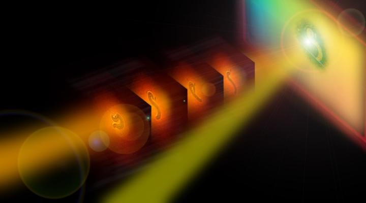
The team then moved to replace the photodiode with a charge-coupled device (CDD) camera, which also uses silicon as the photosensitive material. Through NTA, they were able to capture MIR-derived images on a 1392×1040 pixel sensor at 100 ms exposure times, yielding chemically selective images of several polymer and biological materials as well as living nematodes. Despite using technology not specifically optimized for NTA, the team observed the ability to detect small (10-2) changes in optical density (OD) in the image.
“We are excited to offer this new detection strategy to those who use MIR light for imaging,” says David Knez, one of the team members. “We have high hopes that the simplicity and versatility of this approach allows for the broad adoption and development of the technology.” Adding that NTA may speed up analysis in a wide variety of fields, such as pharmaceutical quality assurance, geologic mineral sampling, or microscopic inspection of biological samples.
###
Media Contact
Dmitry Fishman
[email protected]
Related Journal Article
http://dx.


