Study co-led by Berkeley Lab reveals how wavelike plasmons could power up a new class of sensing and photochemical technologies at the nanoscale
Credit: Felipe da Jornada/Berkeley Lab
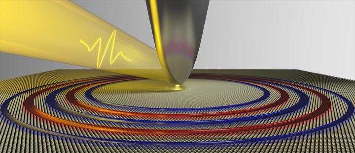
Wavelike, collective oscillations of electrons known as “plasmons” are very important for determining the optical and electronic properties of metals.
In atomically thin 2D materials, plasmons have an energy that is more useful for applications, including sensors and communication devices, than plasmons found in bulk metals. But determining how long plasmons live and whether their energy and other properties can be controlled at the nanoscale (billionths of a meter) has eluded many.
Now, as reported in the journal Nature Communications, a team of researchers co-led by the Department of Energy’s Lawrence Berkeley National Laboratory (Berkeley Lab) – with support from the Department of Energy’s Center for Computational Study of Excited-State Phenomena in Energy Materials (C2SEPEM) – has observed long-lived plasmons in a new class of conducting transition metal dichalcogenide (TMD) called “quasi 2D crystals.”
To understand how plasmons operate in quasi 2D crystals, the researchers characterized the properties of both nonconductive electrons as well as conductive electrons in a monolayer of the TMD tantalum disulfide. Previous studies only looked at conducting electrons. “We discovered that it was very important to carefully include all the interactions between both types of electrons,” said C2SEPEM Director Steven Louie, who led the study. Louie also holds titles as senior faculty scientist in the Materials Sciences Division at Berkeley Lab and professor of physics at UC Berkeley.
The researchers developed sophisticated new algorithms to compute the material’s electronic properties, including plasmon oscillations with long wavelengths, “as this was a bottleneck with previous computational approaches,” said lead author Felipe da Jornada, who was a postdoctoral researcher in Berkeley Lab’s Materials Sciences Division at the time of the study. Jornada is currently an assistant professor in materials science and engineering at Stanford University.
To the researchers’ surprise, the results from calculations performed by the Cori supercomputer at Berkeley Lab’s National Energy Research Scientific Computing Center (NERSC) revealed that plasmons in quasi 2D TMDs are much more stable – for as long as approximately 2 picoseconds, or 2 trillionths of a second – than previously thought.
Their findings also suggest that plasmons generated by quasi 2D TMDs could enhance the intensity of light by more than 10 million times, opening the door for renewable chemistry (chemical reactions triggered by light), or the engineering of electronic materials that can be controlled by light.
In future studies, the researchers plan to investigate how to harness the highly energetic electrons released by such plasmons upon decay, and if they can be used to catalyze chemical reactions.
###
Lede Xian and Angel Rubio of the Max Planck Institute for the Structure and Dynamics of Matter in Hamburg, Germany, contributed to the study.
NERSC is a DOE Office of Science User Facility located at Berkeley Lab.
This study was supported by the Center for Computational Study of Excited-State Phenomena in Energy Materials (C2SEPEM) funded by the U.S. Department of Energy, Office of Basic Energy Sciences. Additional support was provided by the National Science Foundation and the European Research Council.
Additional Information:
“When Plasmons Reach Atomic Flatland,” Max Planck Institute for the Structure and Dynamics of Matter
Founded in 1931 on the belief that the biggest scientific challenges are best addressed by teams, Lawrence Berkeley National Laboratory and its scientists have been recognized with 13 Nobel Prizes. Today, Berkeley Lab researchers develop sustainable energy and environmental solutions, create useful new materials, advance the frontiers of computing, and probe the mysteries of life, matter, and the universe. Scientists from around the world rely on the Lab’s facilities for their own discovery science. Berkeley Lab is a multiprogram national laboratory, managed by the University of California for the U.S. Department of Energy’s Office of Science.
DOE’s Office of Science is the single largest supporter of basic research in the physical sciences in the United States, and is working to address some of the most pressing challenges of our time. For more information, please visit energy.gov/science.
Media Contact
Theresa Duque
[email protected]
Original Source
https:/
Related Journal Article
http://dx.


