Credit: by Tze Chien Sum
Producing clean energy and reducing the power consumption of illumination and personal devices are key challenges to reduce the impact of modern civilization on the environment. As a result, the surging demand for solar cells and light-emitting devices is driving scientists to explore new semiconductor materials and improve their performances, while lowering the production costs.
Semiconductor nanocrystals (materials with sizes about 10 nanometers, which is approximately 10,000 times thinner than our hair) hold great promise for these applications: they are cheap to produce, can be easily integrated in these devices and possess exceptionally enhanced properties upon interaction with the light, as compared to their bulk counterparts. This strong coupling with light gives them a distinctive edge over conventional semiconductors, thus paving the way to high efficiency devices.
Unfortunately, this edge comes at a cost: when the size of a semiconductor is reduced, electrons can no longer travel freely across the material constrained by their physical dimensions. Furthermore, their much larger surfaces necessitate the use of passivation strategies (e.g., with organic ligands) to reduce the traps that could inadvertently affect the charge transport even further. Therefore, practical wide-spread applications of nanocrystals are limited, and their disruptive potential cannot be exploited.
In a new paper published in Light: Science & Application, a team of scientists, led by Professor Tze Chien Sum from Nanyang Technological University (NTU), Singapore, have discovered that nanocrystals made of halide perovskites possess extraordinary properties of energy transport, which replace the transport of charges, and could open new venues for implementing these materials in high efficiency devices.
Prof. Sum and his team have already pioneered the study of charge transport in these materials. In 2013 the team reported unprecedented electron transport properties for bulk halide perovskites and this discovery underpinned the successes of halide perovskites in the following years.
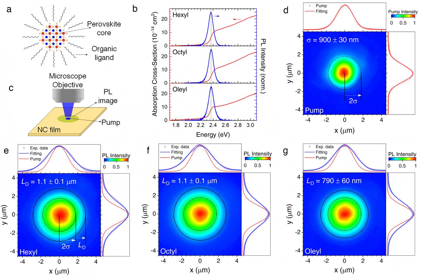
In this work, Prof. Sum’s team demonstrated that surprisingly energy can be transported very efficiently in films made of nanocrystals. The team used a microscopy imaging system to “visualize” the energy traveling using their strong light-emission as a probe, as shown in Figure 1.
While negative and positive charges (electrons and holes, respectively) alone cannot travel inside this nanostructured material, they can team up and form so-called “excitons” to travel together, as shown in the Figure 2. The energy mobility in these materials exceeds that of other conventional nanostructures, such as Cadmium Selenide (CdSe) quantum dots by more than 1 order of magnitude. Moreover, energy can even travel in these materials further compared to what charges can do in bulk halide perovskites.
“This result is unprecedented. When you reduce the size of a material, usually it means you reduce the maximum distance that the charges can travel inside it. However, in halide perovskites, when you reduce their dimension to quantum size, these charges manage to arrange themselves into excitons and find a different way to travel. Their range now is even for longer distance than their initial travel range before you reduce their sizes!” said Dr. David Giovanni and Dr. Marcello Righetto, two of the lead authors of the work who shared equal contributions.
Here, two energy transport mechanisms were identified: the excitons “jump” very effectively between different nanocrystals, and their transport is assisted by emission light being trapped within the film and therefore reabsorbed. For the first time, scientist provided a method to distinguish these two contributions.
While the next challenge to directly implement these extraordinary properties for actual devices still remains (i.e., excitons have to be split in positive and negative charges to create a detectable current), this discovery of long-range energy transport and their mechanisms provide new ways of exploiting nanostructures into devices.
###
Media Contact
Tze Chien Sum
[email protected]
Related Journal Article
http://dx.

