Metallic surfaces no longer protected as topological insulators become thinner
Credit: Lisa Potter/University of Utah
Quantum computers promise to perform operations of great importance believed to be impossible for our technology today. Current computers process information via transistors carrying one of two units of information, either a 1 or a 0. Quantum computing is based on the quantum mechanical behavior of the logic unit. Each quantum unit, or “qubit,” can exist in a quantum superposition rather than taking discrete values. The biggest hurdles to quantum computing are the qubits themselves–it is an ongoing scientific challenge to create logic units robust enough to carry instructions without being impacted by the surrounding environment and resulting errors.
Physicists have theorized that a new type of material, called a three-dimensional (3-D) topological insulator (TI), could be a good candidate from which to create qubits that will be resilient from these errors and protected from losing their quantum information. This material has both an insulating interior and metallic top and bottom surfaces that conduct electricity. The most important property of 3-D topological insulators is that the conductive surfaces are predicted to be protected from the influence of the surroundings. Few studies exist that have experimentally tested how TIs behave in real life.
A new study from the University of Utah found that in fact, when the insulating layers are as thin as 16 quintuple atomic layers across, the top and bottom metallic surfaces begin to influence each other and destroy their metallic properties. The experiment demonstrates that the opposite surfaces begin influencing each other at a much thicker insulating interior than previous studies had shown, possibly approaching a rare theoretical phenomenon in which the metallic surfaces also become insulating as the interior thins out.
“Topological insulators could be an important material in future quantum computing. Our findings have uncovered a new limitation in this system,” said Vikram Deshpande, assistant professor of physics at the University of Utah and corresponding author of the study. “People working with topological insulators need to know what their limits are. It turns out that as you approach that limit, when these surfaces start “talking” to each other, new physics shows up, which is also pretty cool by itself.”
The new study published on July 16, 2019 in the journal Physics Review Letters.
Sloppy sandwiches built from topological insulators
Imagine a hardcover textbook as a 3-D topological insulator, Deshpande said. The bulk of the book are the pages, which is an insulator layer–it can’t conduct electricity. The hardcovers themselves represent the metallic surfaces. Ten years ago, physicists discovered that these surfaces could conduct electricity, and a new topological field was born.
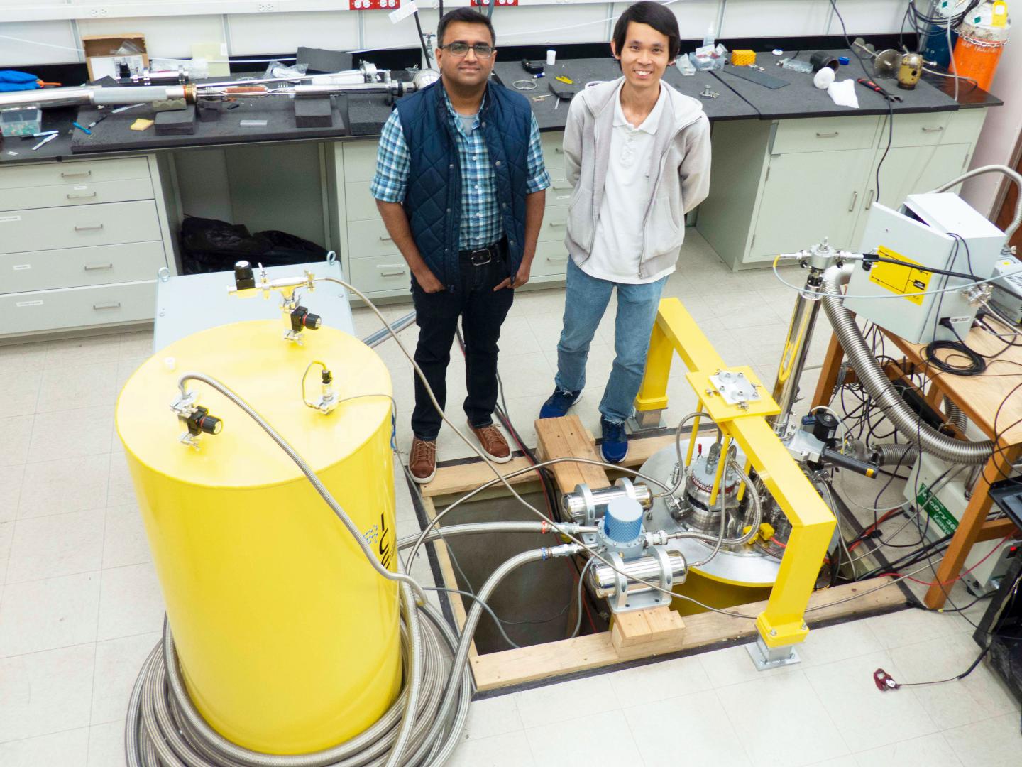
Deshpande and his team created devices using 3-D TIs by stacking five few-atom-thin layers of various materials into sloppy sandwich-like structures. The bulk core of the sandwich is the topological insulator, made from a few quintuple layers of bismuth antimony tellurium selenide (Bi2-xSbxTe3-ySey). This core is sandwiched by a few layers of boron nitride, and is topped off with two layers of graphite, above and below. The graphite works like metallic gates, essentially creating two transistors that control conductivity. Last year Deshpande led a study that showed that this topological recipe built a device that behaved like you would expect – bulk insulators that protect the metallic surfaces from the surrounding environment.
In this study, they manipulated the 3-D TI devices to see how the properties changed. First, they built van der Waal heterostructures–those sloppy sandwiches–and exposed them to a magnetic field. Deshpande’s team tested many at his lab at the University of Utah and first author Su Kong Chong, doctoral candidate at the U, traveled to the National High Magnetic Field Lab in Tallahassee to perform the same experiments there using one of the highest magnetic fields in the country. In the presence of the magnetic field, a checkerboard pattern emerged from the metallic surfaces, showing the pathways by which electrical current will move on the surface. The checkerboards, consisting of quantized conductivities versus voltages on the two gates, are well-defined, with the grid intersecting at neat intersection points, allowing the researchers to track any distortion on the surface.
They began with the insulator layer at 100 nanometers thick, about a thousandth of the diameter of a human hair, and progressively got thinner down to 10 nanometers. The pattern started distorting until the insulator layer was at 16 nanometers thick, when the intersection points began to break up, creating a gap that indicated that the surfaces were no longer conductive.
“Essentially, we’ve made something that was metallic into something insulating in that parameter space. The point of this experiment is that we can controllably change the interaction between these surfaces,” said Deshpande. “We start out with them being completely independent and metallic, and then start getting them closer and closer until they start ‘talking,’ and when they’re really close, they are essentially gapped out and become insulating.”
Previous experiments in 2010 and 2012 had also observed the energy gap on the metallic surfaces as the insulating material thins out. But those studies concluded that the energy gap appeared with much thinner insulating layers–five nanometers in size. This study observed the metallic surface properties break down at much larger interior thickness, up to 16 nanometers. The other experiments used different “surface science” methods where they observed the materials through a microscope with a very sharp metallic tip to look at every atom individually or studied them with highly energetic light.
“These were extremely involved experiments which are pretty far removed from the device-creation that we are doing,” said Deshpande.
Next, Deshpande and the team will look more closely into the physics creating that energy gap on the surfaces. He predicts that these gaps can be positive or negative depending on material thickness.
###
Other authors who contributed to the study are Kyu Bum Han and Taylor Sparks from the U’s Department of Materials Science and Engineering.
Media Contact
Lisa Potter
[email protected]
Original Source
http://unews.
Related Journal Article
http://dx.


