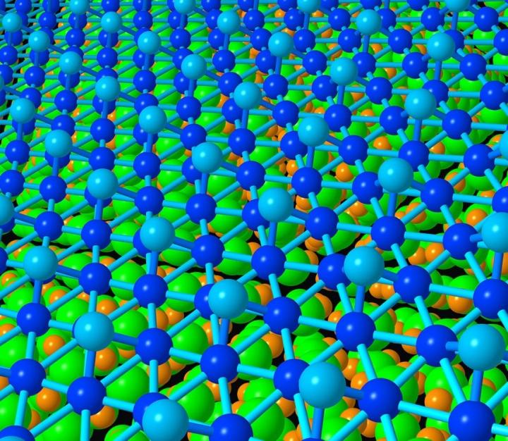
Scientists reveal ‘flat band’ behavior in 2D ‘bitriangular’ lattice of germanium, confirming earlier theoretical prediction
Credit: JAIST
Scientists have recently revealed, both theoretically and experimentally, that germanium atoms can arrange themselves into a 2D “bitriangular” lattice on zirconium diboride thin films grown on germanium single crystals to form a “flat band material” with an embedded “kagome” lattice. The result provides experimental support to a theoretical prediction of flat bands emerging from trivial atomic geometry and indicates the possibility of their existence in many more materials.
The human mind is naturally drawn to objects that possess symmetry; in fact, the notion of beauty is often conflated with symmetry. In nature, nothing epitomizes symmetry more than crystals. Since their discovery, crystals have attracted a great deal of attention not only by their unique “symmetrical” aesthetic appeal but also by their unique properties. One of these properties is the behavior of electrons inside a crystal. From a physical point of view, an electron within a crystal can be fully characterized by its energy and a quantity called “crystal momentum,” which relates to how fast the electron moves in a crystal. The relationship between the energy and crystal momentum of electrons is what scientists refer to as “band structure,” which, put simply, is the allowed energy levels for the electrons within the crystal.
Recently, materials scientists have turned their attention towards what are called “flat band materials”–a class of materials possessing a band structure in which the energy does not vary with the crystal momentum and hence resembles a flat line when plotted as a function of crystal momentum–owing to their ability to give rise to exotic states of matter, such as ferromagnetism (iron-like spontaneous magnetism) and superconductivity (zero resistance to electricity flow). Generally, these “flat bands” are observed in special 2D structures that go by names like “checkerboard lattice,” “dice lattice,” “kagome lattice,” etc. and are typically observed either within the crystal or at the surface of layered materials. A pertinent question thus presents itself–is it possible to embed such lattices into completely new 2D structures? Efforts to design 2D materials have focused on answering this question, and a recent finding suggests that the answer is a “yes.”
Now, in a study published in Physical Review B as a Rapid Communication, an international team of scientists from the Japan Advanced Institute of Science and Technology (JAIST), the University of Tokyo, the Japan Atomic Energy Agency, and Institute for Molecular Science in Japan and Tamkang University in Taiwan, led by Dr. Antoine Fleurence and Prof. Yukiko Yamada-Takamura, has reported a possible new flat band material obtained from germanium (Ge) atoms arranging themselves into a 2D “bitriangular” lattice on zirconium diboride thin films grown on germanium single crystals. The published study is also trending as a #PRBTopDownload on the official Physical Review B handle on Twitter: https:/
Last year, a part of the team published a theoretical paper in the same journal underlining the conditions under which a 2D “bitriangular” lattice can form a flat band. They found that this is related to a “kagome” (meaning weaved basket pattern in Japanese) lattice–a term originally coined by Japanese physicists in the ’50s to study magnetism. “I was really excited when I found out that the electronic structure of kagome lattice can be embedded into a very different-looking 2D structure”, recalls Prof. Chi-Cheng Lee, a physicist at Tamkang University, Taiwan, involved in the study, who predicted the presence of flat bands in the “bitriangular” lattice.
The prediction was finally confirmed after the team, in their current study, characterized the prepared 2D material using various techniques such as scanning tunneling microscopy, positron diffraction, and core-level and angle-resolved photoelectron emission; and backed up the experimental data with theoretical calculations to reveal the underlying “bitriangular” lattice.
“The result is really exciting as it shows that flat bands can emerge even from trivial structures and can possibly be realized in many more materials. Our next step is to see what happens at low temperature, and how it is related to the flat bands of the Ge bitriangular lattice,” says Dr. Fleurence, who is also the first author of this paper.
Indeed, who would’ve thought that a typical, run-of-the-mill semiconductor like germanium could offer such exotic and unprecedented possibilities? The 2D world might have more surprises up its sleeve than we imagine.
###
About Japan Advanced Institute of Science and Technology, Japan
Founded in 1990 in Ishikawa prefecture, the Japan Advanced Institute of Science and Technology (JAIST) was the first independent national graduate school in Japan. Now, after 30 years of steady progress, JAIST has become one of Japan’s top-ranking universities. JAIST counts with multiple satellite campuses and strives to foster capable leaders with a state-of-the-art education system where diversity is key; about 40% of its alumni are international students. The university has a unique style of graduate education based on a carefully designed coursework-oriented curriculum to ensure that its students have a solid foundation on which to carry out cutting-edge research. JAIST also works closely both with local and overseas communities by promoting industry-academia collaborative research.
About Dr. Antoine Fleurence from Japan Advanced Institute of Science and Technology, Japan
Dr. Antoine Fleurence is a Senior Lecturer in the School of Materials Science at Japan Advanced Institute of Science and Technology (JAIST), Japan, since 2018. He received his M.S. and PhD from the University of Paris-Sud in 2004 and 2007, respectively. He was a postdoctoral fellow at JAIST from 2009 to 2012 and served there as Assistant Professor from 2012 to 2018. He specializes in thin-film surfaces and interfaces. His research interests include 2D materials, surface science, and growth of inorganic thin films.
About Professor Yukiko Yamada-Takamura from Japan Advanced Institute of Science and Technology, Japan
Dr. Yukiko Yamada-Takamura is a Professor in the School of Materials Science at the Japan Advanced Institute of Science and Technology (JAIST), Japan, since 2020. She received her PhD from the University of Tokyo in 1998. She was a research associate at Tohoku University from 2002-2006. She joined JAIST as a lecturer in 2006. She specializes in material fabrication and microstructure control, nanostructure physics,, and nanomaterials. Her research interest lies in thin films, 2D materials, and cutting-edge microscopies.
Media Contact
Yukiko Yamada-Takamura
[email protected]
Related Journal Article
http://dx.


