University of Minnesota study opens up possibilities for new transparent materials that conduct electricity
Credit: Mkhoyan Group, University of Minnesota
In groundbreaking materials research, a team led by University of Minnesota Professor K. Andre Mkhoyan has made a discovery that blends the best of two sought-after qualities for touchscreens and smart windows–transparency and conductivity.
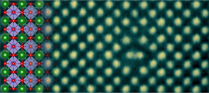
The researchers are the first to observe metallic lines in a perovskite crystal. Perovskites abound in the Earth’s center, and barium stannate (BaSnO3) is one such crystal. However, it has not been studied extensively for metallic properties because of the prevalence of more conductive materials on the planet like metals or semiconductors. The finding was made using advanced transmission electron microscopy (TEM), a technique that can form images with magnifications of up to 10 million.
The research is published in Science Advances, a peer-reviewed scientific journal published by the American Association for the Advancement of Science (AAAS).
“The conductive nature and preferential direction of these metallic line defects mean we can make a material that is transparent like glass and at the same time very nicely directionally conductive like a metal,” said Mkhoyan, a TEM expert and the Ray D. and Mary T. Johnson/Mayon Plastics Chair in the Department of Chemical Engineering and Materials Science at the University of Minnesota’s College of Science and Engineering. “This gives us the best of two worlds. We can make windows or new types of touch screens transparent and at the same time conductive. This is very exciting.”
Defects, or imperfections, are common in crystals–and line defects (the most common among them is the dislocation) are a row of atoms that deviate from the normal order. Because dislocations have the same composition of elements as the host crystal, the changes in electronic band structure at the dislocation core, due to symmetry-reduction and strain, are often only slightly different than that of the host. The researchers needed to look outside the dislocations to find the metallic line defect, where defect composition and resulting atomic structure are vastly different.
“We easily spotted these line defects in the high-resolution scanning transmission electron microscopy images of these BaSnO3 thin films because of their unique atomic configuration and we only saw them in the plan view,” said Hwanhui Yun, a graduate student in the Department of Chemical Engineering and Materials Science and a lead author of the study.
For this study, BaSnO3 films were grown by molecular beam epitaxy (MBE)–a technique to fabricate high-quality crystals–in a lab at the University of Minnesota Twin Cities. Metallic line defects observed in these BaSnO3 films propagate along film growth direction, which means researchers can potentially control how or where line defects appear–and potentially engineer them as needed in touchscreens, smart windows, and other future technologies that demand a combination of transparency and conductivity.
“We had to be creative to grow high-quality BaSnO3 thin films using MBE. It was exciting when these new line defects came into light in the microscope,” said Bharat Jalan, associate professor and Shell Chair in the Department of Chemical Engineering and Materials Science, who heads up the lab that grows a variety of perovskite oxide films by MBE.
Perovskite crystals (ABX3) contain three elements in the unit cell. This gives it freedom for structural alterations such as composition and crystal symmetry, and the ability to host a variety of defects. Because of different coordination and bonding angles of the atoms in the line defect core, new electronic states are introduced and the electronic band structure is modified locally in such a dramatic way that it turns the line defect into metal.
“It was fascinating how theory and experiment agreed with each other here,” said Turan Birol, assistant professor in the Department of Chemical Engineering and Materials Science and an expert in density functional theory (DFT). “We could verify the experimental observations of the atomic structure and electronic properties of this line defect with first principles DFT calculations.”
###
Members of the research team include University of Minnesota Ph.D. students and postdoctoral fellows Hwanhui Yun, Mehmet Topsakal (now associate scientist at Brookhaven National Laboratory), and Abhinav Prakash (postdoc researcher Argonne National Laboratory); and University of Minnesota faculty members K. Andre Mkhoyan, Bharat Jalan, Turan Birol, and Jong Seok Jeong.
This research was supported in part by SMART, one of seven centers of nCORE, a Semiconductor Research Corporation program, sponsored by National Institute of Standards and Technology, and by the National Science Foundation (NSF) through the University of Minnesota Materials Research Science and Engineering Center (MRSEC). The team also worked with the University of Minnesota Characterization Facility. The MBE growth work was supported partially by the NSF and the Air Force Office of Scientific Research.
Media Contact
University of Minnesota Public Relations
[email protected]
Original Source
https:/
Related Journal Article
http://dx.


