• HOME
  • NEWS
  • EXPLORE
    • CAREER
      • Companies
      • Jobs
    • EVENTS
    • iGEM
      • News
      • Team
    • PHOTOS
    • VIDEO
    • WIKI
  • BLOG
  • COMMUNITY
    • FACEBOOK
    • INSTAGRAM
    • TWITTER
Thursday, August 21, 2025
BIOENGINEER.ORG
No Result
View All Result
  • Login
  • HOME
  • NEWS
  • EXPLORE
    • CAREER
      • Companies
      • Jobs
        • Lecturer
        • PhD Studentship
        • Postdoc
        • Research Assistant
    • EVENTS
    • iGEM
      • News
      • Team
    • PHOTOS
    • VIDEO
    • WIKI
  • BLOG
  • COMMUNITY
    • FACEBOOK
    • INSTAGRAM
    • TWITTER
No Result
View All Result
Bioengineer.org
No Result
View All Result
Home NEWS Science News Chemistry

Color superlensing to assist in surpassing diffraction barrier

Bioengineer by Bioengineer
January 3, 2020
in Chemistry
Reading Time: 2 mins read
0
Share on FacebookShare on TwitterShare on LinkedinShare on RedditShare on Telegram

A paper by Kazan Federal University’s Sergey Kharintsev appeared in Optics Letters

IMAGE

Credit: Kazan Federal University


The research was supported by a Russian Science Foundation’s grant under the title “Synthesis and research of a new class of nanocomposite ceramics with degenerate dielectric permeability for opto-plasmonic applications.”

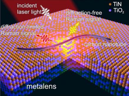
A metalens described in the article is a thin composite metal-dielectric film placed on a dielectric substrate; the width is several dozen nanometers.

“The light has a wave nature, so there is a diffraction limit which confines the resolution of traditional optical microscopy,” explains Kharintsev. “Our metalens is an optical device capable of surpassing that diffraction limit. Such a solution paves way for using optical technologies in nanoscale integral circuits and sensors.”

The ultra-high resolution is based on an unusual behavior of the metalens in optical and infrared ranges.

“The material part of the dielectric constant oscillates near zero. This property can be used to enhance stimulated Raman scattering of light in a spatially limited medium illuminated by low-intensity continuous laser light. For most materials found in nature, nonlinear effects are weak, and to observe them it is necessary to increase the length of the medium (for example, using optical fibers) and / or to increase the laser pump power (using high-power pulsed lasers).

“We used a 50 nm thick titanium oxy nitride (TiON) film as a disordered nonlinear medium. The film was synthesized by magnetron sputtering and subsequent oxidation in air. As a result of a two-stage procedure, metal (TiN) and dielectric (TiO2) nanoparticles were formed in the film. An increase in the amplitude of the Stokes wave in a TiN / TiO2 film occurs due to the enhancement of the cubic susceptibility because of localized plasmon resonance and a small refractive index of the effective medium. Such metal-insulator nanocomposite films having several epsilon-near-zero frequencies in the visible and infrared ramges have found application in creating broadband metal technologies providing resolution beyond the limits of light diffraction,” adds the author.

Kazan University employees have succeeded in visualizing 40 nm multiwall carbon nanotubes scattered along the surface of the metalens created by them, and the resolution was below 100 nm.

“Nanocomposite epsilon-near-zero film works as a surface-enhanced Raman scattering substrate, and it helps not only enhance the scattered signal, but also achieve beyond-diffraction resolutions. Metalenses and ENZ films can be used to create broadband absorbers for solar panels,” concludes Dr. Kharintsev.

###

Media Contact
Yury Nurmeev
[email protected]

Original Source

https://kpfu.ru/eng/news-eng/color-superlensing.html

Related Journal Article

http://dx.doi.org/10.1364/OL.44.005909

Tags: Chemistry/Physics/Materials SciencesMaterialsOptics
Share12Tweet8Share2ShareShareShare2

Related Posts

The Evolution of Metalenses: From Single Devices to Integrated Arrays

The Evolution of Metalenses: From Single Devices to Integrated Arrays

August 21, 2025
Zigzag Graphene Nanoribbons with Porphyrin Edges

Zigzag Graphene Nanoribbons with Porphyrin Edges

August 21, 2025

Bending Light: UNamur and Stanford Unite to Revolutionize Photonic Devices

August 21, 2025

On-Chip All-Dielectric Metasurface Enables Creation of Topological Exceptional Points

August 21, 2025
Please login to join discussion

POPULAR NEWS

  • blank

    Molecules in Focus: Capturing the Timeless Dance of Particles

    141 shares
    Share 56 Tweet 35
  • New Drug Formulation Transforms Intravenous Treatments into Rapid Injections

    114 shares
    Share 46 Tweet 29
  • Neuropsychiatric Risks Linked to COVID-19 Revealed

    81 shares
    Share 32 Tweet 20
  • Modified DASH Diet Reduces Blood Sugar Levels in Adults with Type 2 Diabetes, Clinical Trial Finds

    60 shares
    Share 24 Tweet 15

About

We bring you the latest biotechnology news from best research centers and universities around the world. Check our website.

Follow us

Recent News

STN1 Drives Pancreatic Cancer Metastasis via ZEB1

Anxiety, Anxiety Medications Linked to Parkinson’s Risk

Celebrating 30 Years of Nanoimprint Lithography: Pioneering a New Era in Nanomanufacturing

  • Contact Us

Bioengineer.org © Copyright 2023 All Rights Reserved.

Welcome Back!

Login to your account below

Forgotten Password?

Retrieve your password

Please enter your username or email address to reset your password.

Log In
No Result
View All Result
  • Homepages
    • Home Page 1
    • Home Page 2
  • News
  • National
  • Business
  • Health
  • Lifestyle
  • Science

Bioengineer.org © Copyright 2023 All Rights Reserved.