In the realm of optical technology, lenses have long served as fundamental tools for focusing light and capturing images with precision. From the bulky lenses of early cameras to the compact systems integrated into today’s smartphones, the evolution of lens design reflects a relentless pursuit of miniaturization and enhanced functionality. Nevertheless, traditional lenses inherently demand a certain thickness and curvature to bend light accurately, a physical constraint that poses limits especially in the race towards ever-thinner, lighter portable devices. This challenge has inspired scientists to rethink optics at the nanoscale, leading to the advent of metalenses—ultra-thin, flat lenses capable of performing the same functions as their bulky glass counterparts but with substantially reduced size and weight.
Metalenses represent a radical departure from classical glass optics. Instead of relying on curved glass to refract and focus light, they employ metasurfaces composed of intricately engineered nanostructures. These nanostructures, often mere hundreds of nanometres in size, manipulate light waves by controlling phase, amplitude, and polarization at a scale far below the wavelength of visible light. This nanoscale control enables metalenses to bend and focus light efficiently while being tens of thousands of times thinner than conventional lenses. Such a paradigm shift not only promises to revolutionize consumer electronics by further slimming down camera modules but also opens new horizons for optical applications where space and weight are critical constraints.
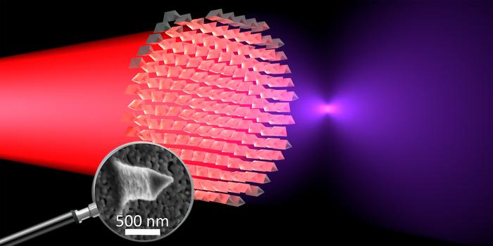
A recent breakthrough in this field has been demonstrated by researchers at ETH Zurich, who have successfully developed a novel method to fabricate metalenses from lithium niobate, a well-known crystalline material with exceptional nonlinear optical properties. Lithium niobate is celebrated for its capacity to alter the frequency of light passing through it—a phenomenon known as nonlinear optics. By converting incoming infrared light into visible wavelengths, this material enables devices that can manipulate light in innovative ways beyond simple focusing. However, until now, shaping lithium niobate into nanostructures suitable for metalenses has been technologically challenging due to its robustness and conventional fabrication difficulties.
.adsslot_iOubeWKBXG{ width:728px !important; height:90px !important; }
@media (max-width:1199px) { .adsslot_iOubeWKBXG{ width:468px !important; height:60px !important; } }
@media (max-width:767px) { .adsslot_iOubeWKBXG{ width:320px !important; height:50px !important; } }
ADVERTISEMENT
The team, led by Professor Rachel Grange, devised a groundbreaking nanoimprinting technique that allows lithium niobate to be molded into the complex metasurfaces required for metalenses efficiently and at scale. This fabrication process ingeniously combines chemical synthesis with precision nanoengineering. The liquid precursor containing lithium niobate’s constituent materials is “stamped” in a manner reminiscent of Gutenberg’s printing press, enabling the creation of nanoscale patterns. Subsequently, the imprinted structures are subjected to controlled heating at 600°C, which crystallizes the material and imparts the desired optical properties necessary for frequency conversion.
This innovative method overcomes several limitations previously associated with the production of lithium niobate nanostructures. Traditional fabrication methods struggled with lithium niobate’s remarkable hardness and chemical stability, often resulting in slow, costly, and labor-intensive manufacturing. The nanoimprinting approach not only significantly reduces production costs and time but also allows the repeated use of inverse molds for mass production, potentially accelerating the commercial deployment of these advanced optical elements.
At the heart of the technology lies the capability of the lithium niobate metalenses to not only focus infrared light sharply but also to convert it into shorter wavelengths of visible light in a highly efficient and controlled manner. When infrared laser light with a wavelength around 800 nanometres passes through the metalens, the nonlinear interactions within the engineered lithium niobate structures generate visible violet light at approximately 400 nanometres, concentrated precisely at the focal point. This unusual ability to combine light focusing with wavelength conversion in an ultra-thin device paves the way for multifaceted photonic systems unparalleled in conventional optics.
The nonlinear optical effect utilized here is not confined to a narrow set of incident light wavelengths. This wavelength-agile characteristic means that these metalenses can be adapted for a wide range of optical frequencies, enhancing their utility in various scientific and industrial contexts. Such flexibility extends the reach of this technology into numerous fields, including telecommunications, microscopy, and advanced sensing, where manipulating light of different wavelengths with high precision is essential.
Beyond traditional uses of lenses, this breakthrough prompts exciting possibilities for security and authentication technologies. The minute nanoscale features integrated into the metalenses make them nearly impossible to replicate without sophisticated manufacturing tools, offering robust counterfeit deterrents. By leveraging the nonlinear optical properties, these metasurfaces can be incorporated into banknotes, documents, or artwork as covert security markers that reliably authenticate their origin under specific illumination conditions.
In practical terms, the use of lithium niobate metalenses promises to simplify the complexity of various optical instruments. For example, sensors that require detecting infrared light—ordinarily invisible to most cameras—can incorporate these metalenses to convert infrared signals into visible light, allowing standard camera systems to perform sophisticated measurements. Moreover, the reduced bulk and enhanced functionality facilitate miniaturized apparatuses in fields such as ultraviolet light patterning for semiconductor manufacturing, potentially revolutionizing how microchips are produced.
This convergence of physics, materials science, and chemistry within the emerging field of metasurface optics is propelling photonic research into uncharted territories. The ETH Zurich team’s accomplishment exemplifies how interdisciplinary approaches can unlock new properties of light and overcome manufacturing challenges to create devices with unprecedented capabilities. Though the field remains in its early days, the impact of scalable, cost-effective nonlinear metalenses is poised to ripple across scientific research, industry, and consumer technology.
Looking forward, the continued development of such metasurfaces suggests the possibility of ultra-compact optical systems that integrate multiple functionalities into a single nanostructured layer. The implications cover not only everyday electronics but also the foundational tools used in quantum computing, optical communication, and biomedical imaging. Researchers are optimistic that these scalable fabrication techniques will catalyze innovations resulting in more sustainable, efficient, and versatile optical devices accessible to a broad spectrum of applications.
Nevertheless, translating laboratory success into commercial products requires addressing challenges such as integrating these metalenses with existing device architectures, optimizing their durability and performance under various operating conditions, and further enhancing their efficiency. Continuous collaboration between material scientists, optical engineers, and industrial partners will be essential for realizing the full potential of this technology, ensuring that the extraordinary properties of lithium niobate metalenses become widely harnessed.
In summarizing this advancement, it is clear that lithium niobate nanoimprinted metalenses mark a significant milestone in nanophotonics. They embody the essence of modern scientific progress by marrying intricate nanoscale engineering with the remarkable intrinsic properties of nonlinear optical materials. As research delves deeper into controlling light with ever-greater finesse, we are set to witness a profound transformation in how imaging, sensing, and light manipulation technologies develop in the near future.
Subject of Research: Not applicable
Article Title: Scalable Lithium Niobate Nanoimprinting for Nonlinear Metalenses
News Publication Date: 14-Apr-2025
Web References: 10.1002/adma.202418957
Image Credits: Ülle-Linda Talts, ETH Zurich
Keywords
Metalenses, lithium niobate, nonlinear optics, nanoimprinting, metasurfaces, nanophotonics, wavelength conversion, infrared to visible light, nanostructures, scalable fabrication, optical miniaturization, advanced materials
Tags: advanced imaging systemsfuture of lens technologyinfrared imaging applicationslightweight lens designmetalenses technologymetasurfaces in photonicsminiaturization in opticsnanoscale optics innovationsnanostructured light manipulationoptical technology breakthroughsultra-thin optical lensesvisualization of infrared light
