Credit: by Yuanhao Mao, Dong Zhao, Shen Yan, Hongjia Zhang, Juan Li, Kai Han, Xiaojun Xu, Chuan Guo, Lexian Yang, Chaofan Zhang, Kun Huang, Yulin Chen
The rapid development of two-dimensional quantum materials, such as twisted bilayer graphene, monolayer copper superconductors, and quantum spin Hall materials, has demonstrated both important scientific implications and promising application potential. To characterize the electronic structure of these materials/devices, angle-resolved photoemission spectroscopy (ARPES) is commonly used to measure the energy and momentum of electrons photoemitted from samples illuminated by X-ray or vacuum ultraviolet (VUV) light sources. Although the X-ray-based spatially resolved ARPES has the highest spatial resolution (~100 nm) benefitting from the relatively short wavelength, its energy resolution is typically mediocre (>10 meV), which makes it difficult to visualize the fine details of the electronic structure in many novel quantum materials. Complementary to X-ray light sources, VUV laser-based light sources can offer much better energy resolution (~0.2 meV), deeper depth of detection and lower cost (compared to synchrotron light sources). However, the longer wavelength of the VUV light source also deteriorates its spatial resolution (typically several micrometres to date), making it insufficient for characterizing small-size flake samples or spatially inhomogeneous (e.g., magnetic, electronic or composite domain) materials.
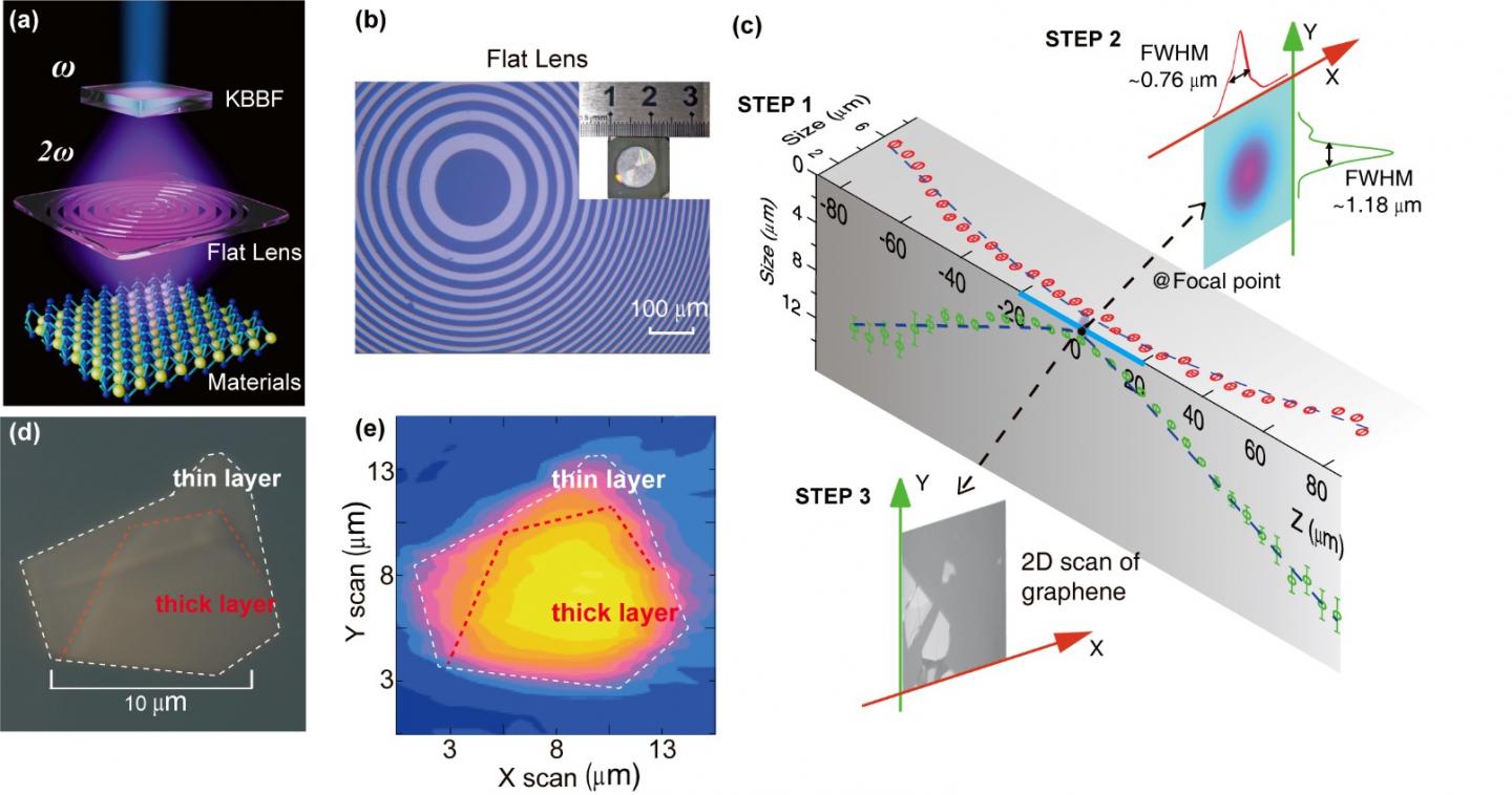
In a new paper published in Light Science & Application, Mao and his co-workers have developed a 177 nm VUV laser system for scanning photoemission microscopy with a focal spot of
Compared with the current DUV laser source with spatial resolution used for ARPES in the world, the 177 nm VUV laser source could help the ARPES measurement cover a larger momentum space and has the better energy resolution, but there are still many challenges and difficulties to make it have excellent spatial resolution:
“First, severe spherical aberration exists in a high-NA refraction lens. Second, only very limited materials can be used in optics for correcting the spherical aberration due to the strong absorption at VUV frequencies. Third, it is practically difficult to check the quality (collimation, uniformity and efficient diameter) of the incident beam and the alignment among optical elements, as the VUV beam is invisible and all optics have to be placed in vacuum or a sealed chamber filled with inert gas.”
This VUV laser focusing system contains five functional parts: a 355 nm laser, a second-harmonic generation stage, a beam shaping stage, a polarization adjustment part and a focusing element of the flat lens.
“To avoid the spherical aberration, we introduce planar diffractive lenses that can realize tight focusing of light by fine tuning of the interference from multiple beams” they added.
“This VUV laser system has ultra-long focal length (~45 mm), sub-micron spatial resolution (~760 nm), ultra-high energy resolution (~0.3 meV) and ultra-high brightness (~355 MWm-2). It can be directly applied to scientific research instruments such as photoemission electron microscopy (PEEM), angle-resolved photoelectron spectrometer (ARPES) and deep ultraviolet laser Raman spectrometer. At present, this system has been connected with the ARPES at ShanghaiTech University revealing the fine energy band features of various new quantum materials such as quasi-one-dimensional topological superconductors TaSe3, magnetic topological insulators (MnBi2Te4)(Bi2Te3)m family, etc.. ” the scientists summarized.
###
Media Contact
Chaofan Zhang
[email protected]
Related Journal Article
http://dx.


