

Researchers Ayten Cantas and Gokhan Yilmaz have demonstrated how post-deposition thermal annealing and environmental stressors alter the electronic defect states, conductivity, and carrier mobility-lifetime products of magnetron-sputtered antimony selenide thin films. Antimony selenide is an earth-abundant, low-toxicity binary chalcogenide semiconductor featuring a direct bandgap between 1.1 and 1.3 electronvolts, an absorption coefficient exceeding 100,000 inverse centimeters, and hole mobility reaching 42 square centimeters per volt-second. Although hydrothermal synthesis has achieved power conversion efficiencies surpassing 11 percent in antimony selenosulfide devices, complex precursor chemistries hinder industrial scaling. By utilizing vacuum-based radio frequency magnetron sputtering on glass substrates, the authors produced dense precursor films to systematically evaluate how an amorphous as-grown film and an annealed crystalline film respond to ambient air, high-purity oxygen, ultraviolet illumination, and broadband light soaking.
Film fabrication was executed by depositing 500-nanometer-thick antimony selenide layers onto soda lime glass substrates from a two-inch target of 99.9 percent purity. The ultra-high-vacuum radio frequency sputtering chamber operated at a base pressure of 4.5 times 10 to the minus six Torr and maintained a working deposition pressure of 1.2 times 10 to the minus three Torr under 30 standard cubic centimeters per minute of pure argon. With the target-to-substrate distance fixed at 8 centimeters, 30 watts of radio frequency power was applied. One specimen was kept in its unheated as-grown state, designated as sample Sb-1. A second specimen, designated as sample Sb-2, underwent thermal crystallization inside a quartz tube furnace under a 100 standard cubic centimeters per minute argon flow, ramped at 20 degrees Celsius per minute to 350 degrees Celsius for 20 minutes.
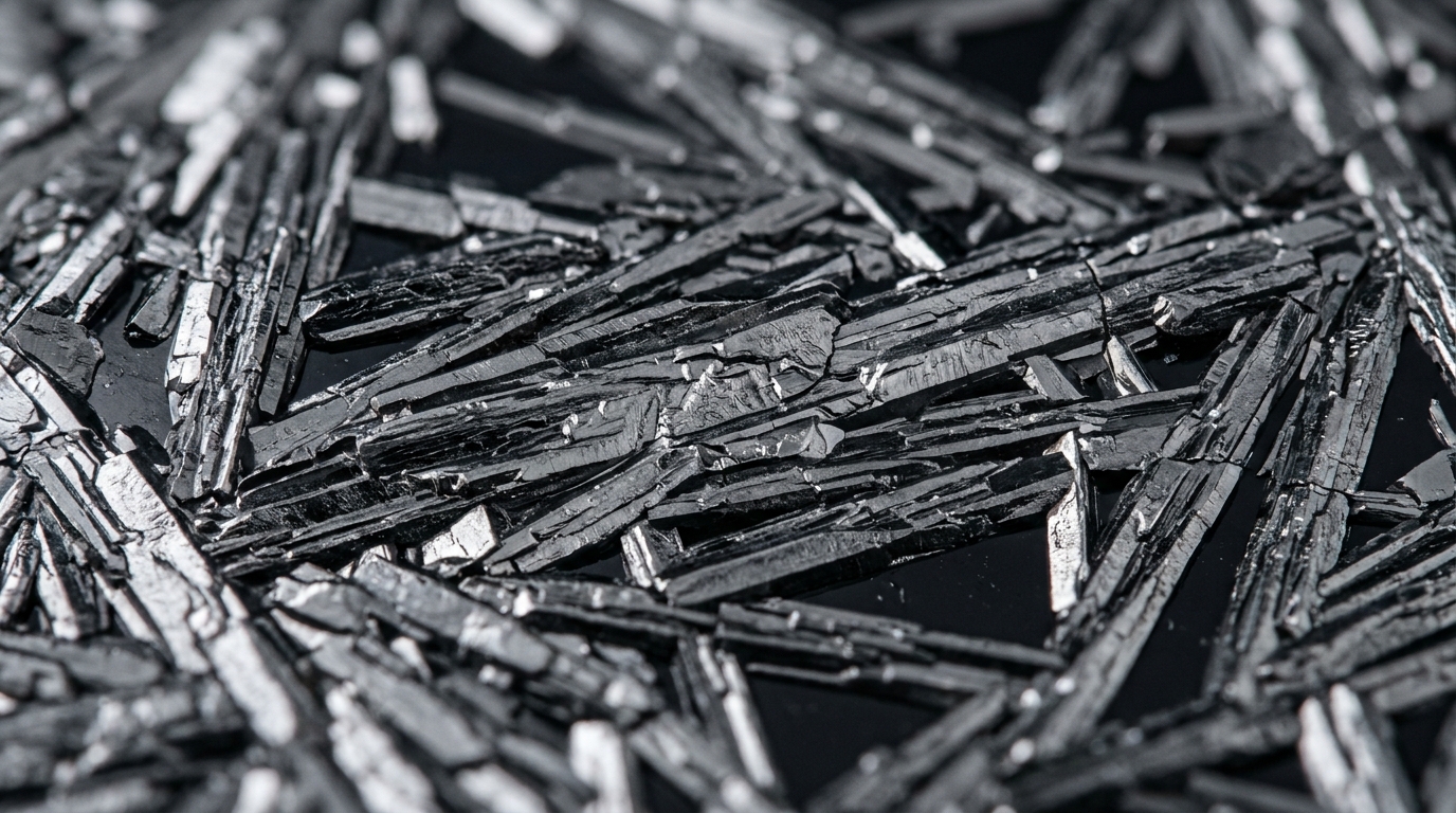
X-ray diffraction analysis using copper K-alpha radiation with a wavelength of 1.5406 angstroms confirmed that as-grown Sb-1 exhibited an amorphous structure lacking resolved diffraction peaks, whereas annealed Sb-2 transformed into a well-defined polycrystalline orthorhombic phase within the Pbnm space group. Antimony selenide possesses a quasi-one-dimensional crystal lattice composed of ribbon chains aligned parallel to the crystallographic c-axis. For photovoltaic applications, efficient charge transport requires ribbon orientations aligned at large angles relative to the substrate surface rather than lying flat against it. While strictly vertical ribbons correspond to (00l) planes, crystallographic reflections fulfilling the empirical criterion where the sum of indices k and l is greater than or equal to three represent favorable, predominantly vertical ribbon orientations. In contrast, planes where the sum of indices h and k is greater than or equal to three denote undesirable lateral growth parallel to the substrate.
To quantitatively assess crystallographic orientation in the annealed Sb-2 film, texture coefficients were calculated across ten high-intensity diffraction peaks: (130), (230), (211), (221), (301), (330), (240), (231), (250), and (061). Although the (221) plane exhibited the highest raw experimental peak intensity, its calculated texture coefficient was 0.73, indicating underrepresentation compared to standard powder diffraction. Instead, texture coefficients markedly exceeding unity were obtained for the (330) plane at 2.17, the (250) plane at 1.75, and the (130) plane at 1.43. All three dominant planes satisfy the vertical alignment condition where the sum of indices k and l is greater than or equal to three. This preferential orientation demonstrates that post-deposition annealing effectively aligned the antimony selenide ribbons at steep angles relative to the substrate, reducing grain-boundary potential barriers and creating microstructural conditions conducive to efficient cross-film carrier transport.
Electrical measurements were carried out using a two-probe co-planar surface geometry rather than complete multi-layer device stacks. Silver electrodes with a contact length of 5 millimeters and an inter-electrode separation gap of 0.5 millimeters were deposited on the film surface, with gold-coated probe tips establishing stable electrical connections. Film thickness was verified across ten positions using a Veeco DEKTAK 150 profilometer, confirming an average thickness of approximately 500 nanometers. Direct-current voltage was applied across the co-planar electrodes while measuring the resulting current, enabling dark conductivity calculations based on applied voltage, measured current, film thickness, contact length, and electrode gap spacing. By omitting bottom electrodes, transparent conductive oxides, and intervening buffer layers, this co-planar configuration eliminated interfacial contact artifacts and heterojunction influences, permitting direct measurement of the intrinsic electrical properties of the antimony selenide films.
All environmental stress testing followed a strict chronological procedure inside a cryostat system at 300 Kelvin. Initial measurements were recorded under ambient laboratory air, after which the system was evacuated to vacuum and subjected to an initial thermal reset annealing step. This reset treatment, denoted as annealing-1, heated the films to 440 Kelvin for 30 minutes under vacuum before cooling at 2 Kelvin per minute back to 300 Kelvin under proportional integral derivative control. Annealing-1 served as the baseline reference state against which all subsequent aging deviations were measured. The chronological cycle continued with ultraviolet irradiation under vacuum followed by a second reset annealing, exposure to high-purity 99.99 percent oxygen followed by a third reset annealing, and broadband light soaking under vacuum followed by a fourth reset annealing, isolating the cumulative impact of each stressor.
Evacuating the cryostat from ambient laboratory atmosphere to vacuum caused the dark conductivity of both amorphous Sb-1 and crystalline Sb-2 films to decrease by nearly one order of magnitude, showing strong sensitivity to atmospheric gas adsorption. When high-purity oxygen was subsequently introduced at 300 Kelvin, dark conductivity rose by approximately a factor of two, while overall oxygen exposure produced an increase of approximately one order of magnitude that reversed upon re-evacuation. The researchers interpret this reversible behavior as physical adsorption or reversible chemisorption of electronegative oxygen molecules on the film surface, capturing electrons or passivating surface states rather than acting as a permanent chemical p-type dopant. Because the quasi-one-dimensional ribbon structure of antimony selenide creates benign grain boundaries with low dangling bond densities, these conductivity shifts reflect surface-dominated interactions rather than bulk lattice damage.
Radiative aging experiments revealed distinct photoresponse dynamics between the two structural phases under illumination and subsequent dark relaxation. During broadband light soaking using a 250-watt halogen lamp calibrated to AM1.5 solar conditions at a 15-centimeter distance, dark conductivity in amorphous Sb-1 increased by nearly three orders of magnitude, but immediately returned to its baseline once illumination ceased. In crystalline Sb-2, light soaking increased conductivity by approximately one and a half orders of magnitude, but left a residual twofold increase in dark conductivity after the light was turned off. Under narrow-band 390-nanometer ultraviolet illumination from a 40-watt light-emitting diode, amorphous Sb-1 displayed a tenfold conductivity increase that fully reversed after irradiation, whereas crystalline Sb-2 showed a threefold increase that also returned to its pre-illumination annealed baseline, demonstrating that amorphous films exhibit stronger transient photosensitivity.
The mobility-lifetime product was determined through steady-state photoconductivity measurements as a function of carrier generation rate across the range of 10 to the 18th power to 10 to the 21st power inverse cubic centimeters per second. Under steady-state illumination, photoconductivity is directly proportional to elementary charge, optical generation rate, and the mobility-lifetime product. In semiconductor defect physics, changes in the mobility-lifetime curve provide diagnostic insight into defect states: if the magnitude of the product shifts while the slope of the curve against generation rate remains constant, the shift indicates a change in electronic defect concentration alone. If both the magnitude and slope change simultaneously, the alteration indicates a transformation in the dominant electronic defect type, signaling a shift in active carrier recombination centers or trapping mechanisms within the bandgap.
Evaluating the mobility-lifetime products between laboratory-aged and first-annealed states showed that annealing increased the product by a factor of 6 in amorphous Sb-1 with an unchanged slope, confirming reduced defect concentration without altering the conduction mechanism. In crystalline Sb-2, annealing decreased the mobility-lifetime product threefold at low generation rates of 10 to the 18th power while matching the curve at high generation rates of 10 to the 21st power, with a slope shift indicating a change in dominant recombination pathways. Following ultraviolet irradiation, Sb-1 suffered a 1.5-fold decrease in mobility-lifetime product that fully recovered after the second annealing. For crystalline Sb-2, ultraviolet exposure produced an initial twofold increase, which evolved after the second annealing into a persistent threefold increase at low generation rates with an increased slope, demonstrating permanent alteration of dominant conduction mechanisms.
Oxygen exposure produced slight, fully reversible mobility-lifetime shifts in amorphous Sb-1 after the third annealing, but left non-recoverable shifts in crystalline Sb-2 at low generation rates, indicating irreversible deep-level defect redistribution. Under light soaking, Sb-1 maintained its mobility-lifetime values during illumination but exhibited a threefold decline after the fourth annealing due to thermal cycling. Conversely, light-soaked crystalline Sb-2 showed a threefold mobility-lifetime increase that partially relaxed after the fourth annealing, confirming the activation of metastable electronic states. Because characterizations were conducted without carrier-type measurements like Seebeck or capacitance-voltage profiling, surface adsorption mechanisms remain speculative until verified by photoelectron spectroscopy. Nevertheless, these findings demonstrate that crystalline antimony selenide exhibits irreversible environmental defect dynamics, showing that commercial solar cell reliability strictly requires precise ribbon orientation control and robust barrier encapsulation to block ambient oxygen and radiative degradation.
Subject of Research: Phase transitions and environmental defect evolution in antimony selenide thin films
Article Title: Evolution of electronic defect states in sb2se3 thin films: ımpact of phase transition and environmental aging
Article References: Cantas, A., & Yilmaz, G. (2026). Evolution of electronic defect states in sb2se3 thin films: ımpact of phase transition and environmental aging. Applied Physics B, 132(6), Article 77. https://doi.org/10.1007/s00340-026-08686-1
Image Credits: AI Generated
DOI: 10.1007/s00340-026-08686-1
Keywords: antimony selenide, thin films, magnetron sputtering, phase transitions, defect states, environmental aging, photovoltaics, photoconductivity, Evolution, electronic, defect, states
News Source: Gavin Prescott. (November 9, 2026). Antimony Selenide Defect Evolution Under Phase Transitions and Environmental Stressors. Scienmag.