Novel crystal confines electrons to one dimension for spintronic applications

Credit: © 2020 Kondo et al
Spintronics refers to a suite of physical systems which may one day replace many electronic systems. To realize this generational leap, material components that confine electrons in one dimension are highly sought after. For the first time, researchers created such a material in the form of a special bismuth-based crystal known as a high-order topological insulator.
To create spintronic devices, new materials need to be designed that take advantage of quantum behaviors not seen in everyday life. You are probably familiar with conductors and insulators, which permit and restrict the flow of electrons, respectively. Semiconductors are common but less familiar to some; these usually insulate, but conduct under certain circumstances, making them ideal miniature switches.
For spintronic applications, a new kind of electronic material is required and it’s called a topological insulator. It differs from these other three materials by insulating throughout its bulk, but conducting only along its surface. And what it conducts is not the flow of electrons themselves, but a property of them known as their spin or angular momentum. This spin current, as it’s known, could open up a world of ultrahigh-speed and low-power devices.
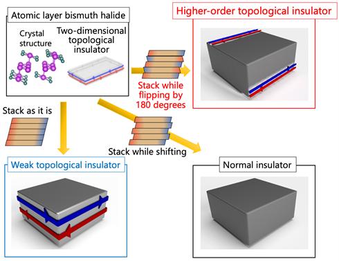
However, not all topological insulators are equal: Two kinds, so-called strong and weak, have already been created, but have some drawbacks. As they conduct spin along their entire surface, the electrons present tend to scatter, which weakens their ability to convey a spin current. But since 2017, a third kind of topological insulator called a higher-order topological insulator has been theorized. Now, for the first time, one has been created by a team at the Institute for Solid State Physics at the University of Tokyo.
“We created a higher-order topological insulator using the element bismuth,” said Associate Professor Takeshi Kondo. “It has the novel ability of being able to conduct a spin current along only its corner edges, essentially one-dimensional lines. As the spin current is bound to one dimension instead of two, the electrons do not scatter so the spin current remains stable.”
To create this three-dimensional crystal, Kondo and his team stacked two-dimensional slices of crystal one atom thick in a certain way. For strong or weak topological insulators, crystal slices in the stack are all oriented the same way, like playing cards face down in a deck. But to create the higher-order topological insulator, the orientation of the slices was alternated, the metaphorical playing cards were faced up then down repeatedly throughout the stack. This subtle change in arrangement makes a huge change in the behavior of the resultant three-dimensional crystal.
The crystal layers in the stack are held together by a quantum mechanical force called the van der Waals force. This is one of the rare kinds of quantum phenomena that you actually do see in daily life, as it is partly responsible for the way that powdered materials clump together and flow the way they do. In the crystal, it adheres the layers together.
“It was exciting to see that the topological properties appear and disappear depending only on the way the two-dimensional atomic sheets were stacked,” said Kondo. “Such a degree of freedom in material design will bring new ideas, leading toward applications including fast and efficient spintronic devices, and things we have yet to envisage.”
###
Journal article
Ryo Noguchi, Masaru Kobayashi, Zhanzhi Jiang, Kenta Kuroda, Takanari Takahashi, Zifan Xu, Daehun Lee, Motoaki Hirayama, Masayuki Ochi, Tetsuroh Shirasawa, Peng Zhang, Chun Lin, Cédric Bareille, Shunsuke Sakuragi, Hiroaki Tanaka, So Kunisada, Kifu Kurokawa, Koichiro Yaji, Ayumi Harasawa, Viktor Kandyba, Alessio Giampietri, Alexei Barinov, Timur K. Kim, Cephise Cacho, Makoto Hashimoto, Donghui Lu, Shik Shin, Ryotaro Arita, Keji Lai, Takao Sasagawa and Takeshi Kondo. Evidence for a higher-order topological insulator in a three-dimensional material built from van der Waals stacking of bismuth-halide chains. Nature Materials. https:/
Funding details
The work done at Tokyo Institute of Technology was supported by a CREST project [JPMJCR16F2] from Japan Science and Technology Agency (JST). This work was supported by the JSPS KAKENHI (grant numbers JP18H01165, JP18J21892, JP18K03484, JP19H02683, JP19F19030 and JP19H00651), and by MEXT Q-LEAP (grant number JPMXS0118068681). This work was also supported by MEXT under the “Program for Promoting Researches on the Supercomputer Fugaku” (Basic Science for Emergence and Functionality in Quantum Matter Innovative Strongly Correlated Electron Science by Integration of “Fugaku” and Frontier Experiments) (Project ID: hp200132).
Institute for Solid State Physics – http://www.
Research contact
Associate Professor Takeshi Kondo
The Institute for Solid State Physics, The University of Tokyo
5-1-5 Kashiwanoha, Kashiwa, Chiba 277-8581 JAPAN
Tel: +81(0)-4-7136-3370
E-mail: [email protected]
Media contact
Mr. Rohan Mehra
Division for Strategic Public Relations, The University of Tokyo
7-3-1 Hongo, Bunkyo-ku, Tokyo 113-8654, JAPAN
Email: [email protected]
About the University of Tokyo
The University of Tokyo is Japan’s leading university and one of the world’s top research universities. The vast research output of some 6,000 researchers is published in the world’s top journals across the arts and sciences. Our vibrant student body of around 15,000 undergraduate and 15,000 graduate students includes over 4,000 international students. Find out more at http://www.
Media Contact
Associate Professor Takeshi Kondo
[email protected]
Original Source
https:/
Related Journal Article
http://dx.


