• HOME
  • NEWS
  • EXPLORE
    • CAREER
      • Companies
      • Jobs
    • EVENTS
    • iGEM
      • News
      • Team
    • PHOTOS
    • VIDEO
    • WIKI
  • BLOG
  • COMMUNITY
    • FACEBOOK
    • INSTAGRAM
    • TWITTER
Thursday, October 8, 2026
BIOENGINEER.ORG
No Result
View All Result
  • Login
  • HOME
  • NEWS
  • EXPLORE
    • CAREER
      • Companies
      • Jobs
        • Lecturer
        • PhD Studentship
        • Postdoc
        • Research Assistant
    • EVENTS
    • iGEM
      • News
      • Team
    • PHOTOS
    • VIDEO
    • WIKI
  • BLOG
  • COMMUNITY
    • FACEBOOK
    • INSTAGRAM
    • TWITTER
  • HOME
  • NEWS
  • EXPLORE
    • CAREER
      • Companies
      • Jobs
        • Lecturer
        • PhD Studentship
        • Postdoc
        • Research Assistant
    • EVENTS
    • iGEM
      • News
      • Team
    • PHOTOS
    • VIDEO
    • WIKI
  • BLOG
  • COMMUNITY
    • FACEBOOK
    • INSTAGRAM
    • TWITTER
No Result
View All Result
Bioengineer.org
No Result
View All Result
Home NEWS Science News Chemistry

2D materials: arrangement of atoms measured in silicene

Bioengineer by Bioengineer
December 23, 2019
in Chemistry
Reading Time: 2 mins read
0
IMAGE
Share on FacebookShare on TwitterShare on LinkedinShare on RedditShare on Telegram

IMAGE

Credit: University of Basel, Department of Physics


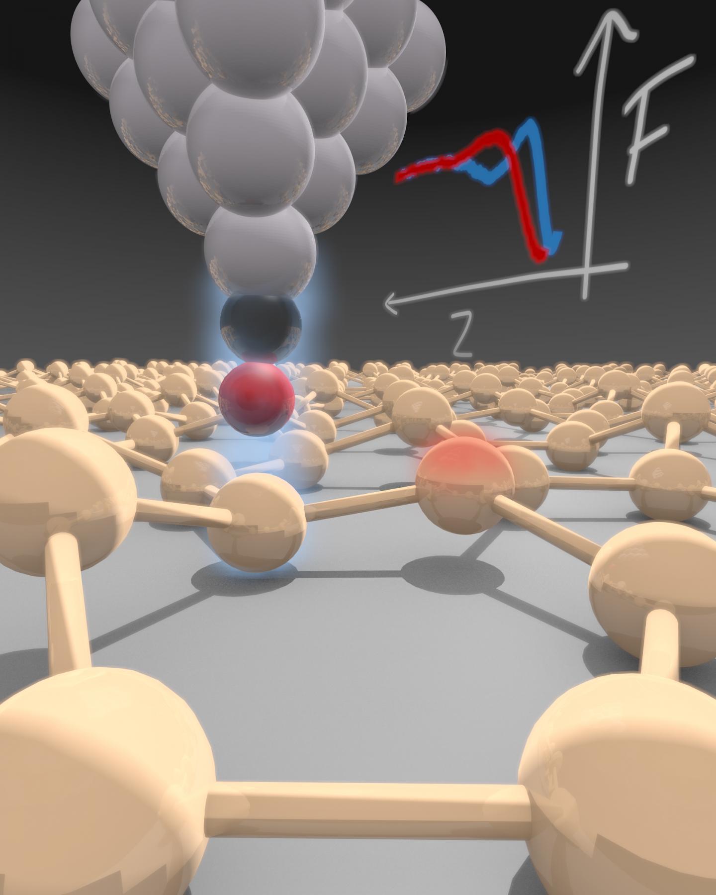
Silicene consists of a single layer of silicon atoms. In contrast to the ultra-flat material graphene, which is made of carbon, silicene shows surface irregularities that influence its electronic properties. Now, physicists from the University of Basel have been able to precisely determine this corrugated structure. As they report in the journal PNAS, their method is also suitable for analyzing other two-dimensional materials.

Since the experimental production of graphene, two-dimensional materials have been at the heart of materials research. Similar to carbon, a single layer of honeycombed atoms can be made from silicon. This material, known as silicene, has an atomic roughness, in contrast to graphene, since some atoms are at a higher level than others.

Silicene not completely flat

Now, the research team, led by Professor Ernst Meyer of the Department of Physics and the Swiss Nanoscience Institute of the University of Basel, has succeeded in quantitatively representing these tiny height differences and detecting the different arrangement of atoms moving in a range of less than one angstrom – that is, less than a 10-millionth of a millimeter.

“We use low-temperature atomic force microscopy with a carbon monoxide tip,” explains Dr. Rémy Pawlak, who played a leading role in the experiments. Force spectroscopy allows the quantitative determination of forces between the sample and the tip. Thus, the height in relation to the surface can be detected and individual atoms can be chemically identified. The measurements show excellent agreement with simulations carried out by partners at the Instituto de Ciencia de Materiales de Madrid (ICMM).

Different electronic properties

This unevenness, known as buckling, influences the electronic properties of the material. Unlike graphene, which is known to be an excellent conductor, on a silver surface silicene behaves more like a semiconductor. “In silicene, the perfect honeycomb structure is disrupted. This is not necessarily a disadvantage, as it could lead to the emergence of interesting quantum phenomena, such as the quantum spin hall effect,” says Meyer.

The method developed by the researchers in Basel offers new insights into the world of two-dimensional materials and the relationship between structure and electronic properties.

###

Media Contact
Dr. Ernst Meyer
[email protected]
41-612-073-724

Related Journal Article

http://dx.doi.org/10.1073/pnas.1913489117

Tags: Atomic/Molecular/Particle PhysicsChemistry/Physics/Materials SciencesMaterials
Share12Tweet8Share2ShareShareShare2

Related Posts

Gelatin Unlocks the Molecular Secrets of 3D-Printed Pork Mince

Gelatin Unlocks the Molecular Secrets of 3D-Printed Pork Mince

October 8, 2026
Chip-Sized Light Rulers Could Carry Atomic Clock Precision Out of the Lab

Chip-Sized Light Rulers Could Carry Atomic Clock Precision Out of the Lab

October 8, 2026

AI Meets Catalysis: A New Scientific Paradigm Is Emerging

October 8, 2026

Invasive Water Hyacinth Transformed Into Pellets That Scrub Dye From Wastewater

October 7, 2026
Please login to join discussion

POPULAR NEWS

  • Alloys That Shrink Their Own Grains: New PIX Mechanism Refines Metals With Heat Alone

    Alloys That Shrink Their Own Grains: New PIX Mechanism Refines Metals With Heat Alone

    29 shares
    Share 12 Tweet 7
  • Endurance Exercise Reshapes the Liver in Males and Females Through Distinct Molecular Routes

    29 shares
    Share 12 Tweet 7
  • Single Transcription Factor PU.1 Rapidly Converts Fibroblasts into Macrophage-Lineage Cells

    29 shares
    Share 12 Tweet 7
  • New Scale Measures How Ready Nurse Educators Really Are for the AI Era

    29 shares
    Share 12 Tweet 7

About

We bring you the latest biotechnology news from best research centers and universities around the world. Check our website.

Follow us

Recent News

Alloys That Shrink Their Own Grains: New PIX Mechanism Refines Metals With Heat Alone

Endurance Exercise Reshapes the Liver in Males and Females Through Distinct Molecular Routes

Single Transcription Factor PU.1 Rapidly Converts Fibroblasts into Macrophage-Lineage Cells

Subscribe to Blog via Email

Success! An email was just sent to confirm your subscription. Please find the email now and click 'Confirm' to start subscribing.

Join 85 other subscribers
  • Contact Us

Bioengineer.org © Copyright 2023 All Rights Reserved.

Welcome Back!

Login to your account below

Forgotten Password?

Retrieve your password

Please enter your username or email address to reset your password.

Log In
No Result
View All Result
  • Homepages
    • Home Page 1
    • Home Page 2
  • News
  • National
  • Business
  • Health
  • Lifestyle
  • Science

Bioengineer.org © Copyright 2023 All Rights Reserved.