Credit: by Nazir Kherani
Through the manipulation of quasiparticles known as surface plasmon polaritons (SPPs) metallic nanostructures can control light at the nanoscale, confining it to ultrathin gaps and magnifying the light intensity up to 1000 times. This light localization amplifies light-matter interactions and has wide ranging applications in nanoscale optics including low concentration molecular sensing, enhanced photocatalysis and super-resolution optics. However, current systems for designing and fabricating these nanostructures lack control over the device’s optical response and often suffer from poor light confinement, limiting the applications which can benefit from this light trapping effect.
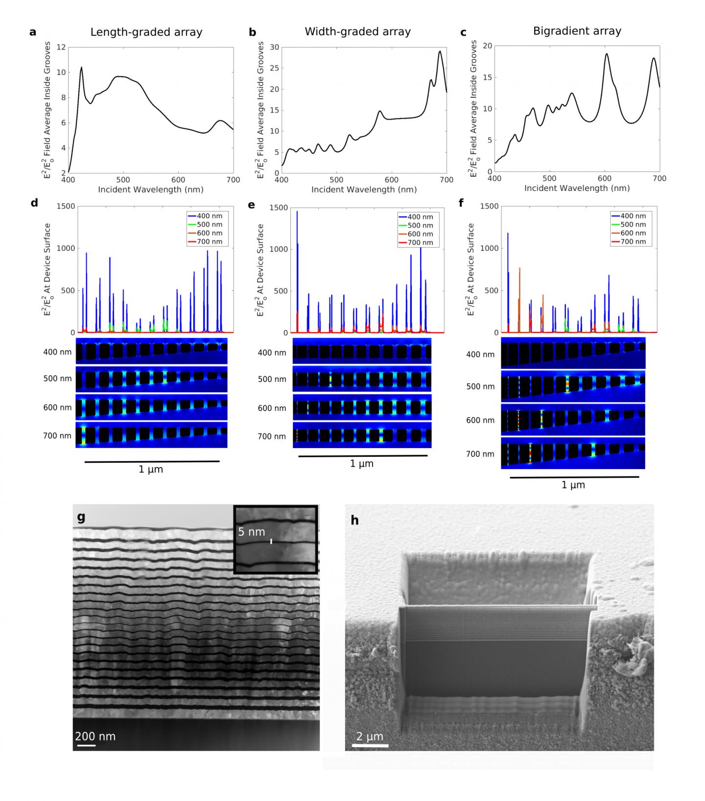
A new paper published in Light Science & Applications from a team of scientists led by Professor Nazir Kherani at the University of Toronto outlines novel design and fabrication techniques optimized for light localization across the visible spectrum, also known as rainbow light trapping. The nanostructures consist of a series of grooves grouped into arrays with gradients in the groove geometry in various configurations providing broadband electromagnetic field enhancement. Using an analytical model combinations of these grooves are designed to produce devices which can control both the spectral and spatial distribution of localized light. The team demonstrated the capabilities of their device design by creating various arrays of ultrathin metallic grooves with groove-widths down to 5 nm, allowing for extreme light confinement. The combination of precise analytical design along with versatile device fabrication and extreme field localization will allow for the ubiquitous application of these structures for the enhancement of many phenomena.
The researchers highlight the versatility of their techniques as key to the significance of their work. “The analytical design approach significantly reduces the time required to develop new devices as compared to the numerous iterative simulations which are currently used. Additionally, the bottom up fabrication technique can be easily modified to create nanostructures for any application while producing very strong electric fields” the scientists state. The researchers hope that this versatility will allow their work to have a wide-ranging impact in the field of nanoscale optics.
###
Media Contact
Nazir Kherani
[email protected]
Related Journal Article
http://dx.


