A new design of ultra-small silicon chip called a multiplexer will effectively manage terahertz waves which are key to the next generation of communications: 6G and beyond
Credit: Osaka University
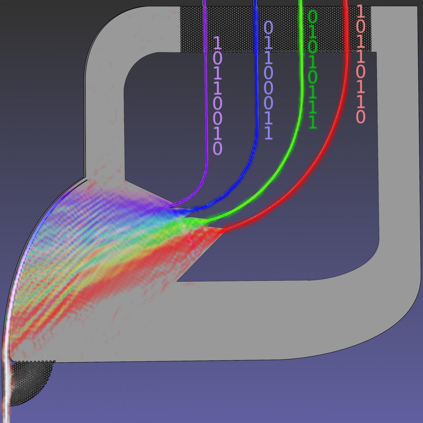
Researchers from Osaka University, Japan and the University of Adelaide, Australia have worked together to produce the new multiplexer made from pure silicon for terahertz-range communications in the 300-GHz band.
“In order to control the great spectral bandwidth of terahertz waves, a multiplexer, which is used to split and join signals, is critical for dividing the information into manageable chunks that can be more easily processed and so can be transmitted faster from one device to another,” said Associate Professor Withawat Withayachumnankul from the University of Adelaide’s School of Electrical and Electronic Engineering.
“Up until now compact and practical multiplexers have not been developed for the terahertz range. The new terahertz multiplexers, which are economical to manufacture, will be extremely useful for ultra-broadband wireless communications.
“The shape of the chips we have developed is the key to combining and splitting channels so that more data can be processed more rapidly. Simplicity is its beauty.”
People around the world are increasingly using mobile devices to access the internet and the number of connected devices is multiplying exponentially. Soon machines will be communicating with each other in the Internet of Things which will require even more powerful wireless networks able to transfer large volumes of data fast.
Terahertz waves are a portion of the electromagnetic spectrum that has a raw spectral bandwidth that is far broader than that of conventional wireless communications, which is based upon microwaves. The team has developed ultra-compact and efficient terahertz multiplexers, thanks to a novel optical tunnelling process.
“A typical four-channel optical multiplexer might span more than 2000 wavelengths. This would be about two meters in length in the 300-GHz band,” said Dr Daniel Headland from Osaka University who is lead author of the study.
“Our device is merely 25 wavelengths across, which offers dramatic size reduction by a factor of 6000.”
The new multiplexer covers a spectral bandwidth that is over 30 times the total spectrum that is allocated in Japan for 4G/LTE, the fastest mobile technology currently available and 5G which is the next generation, combined. As bandwidth is related to data rate, ultra-high-speed digital transmission is possible with the new multiplexer.
“Our four-channel multiplexer can potentially support aggregate data rate of 48 gigabits per second (Gbit/s), equivalent to that of uncompressed 8K ultrahigh definition video being streamed in real time,” said Associate Professor Masayuki Fujita, the team’s leader from Osaka University.
“To make the entire system portable, we plan to integrate this multiplexer with resonant tunnelling diodes to provide compact, multi-channel terahertz transceivers.”
The modulation scheme employed in the team’s study was quite basic; terahertz power was simply switched on-and-off to transmit binary data. More advanced techniques are available that can squeeze even higher data rates towards 1 Terabit/s into a given bandwidth allocation.
“The new multiplexer can be mass-produced, just like computer chips, but much simpler. So large-scale market penetration is possible,” said Professor Tadao Nagatsuma from Osaka University.
“This would enable applications in 6G and beyond, as well as the Internet of Things, and low-probability-of-intercept communications between compact aircraft such as autonomous drones.”
This study, which is published in the journal Optica and was financed by the Japan Science and Technology Agency (JST) CREST funding program, KAKENHI grant, and an Australia Research Council (ARC) Discovery grant, builds on the team’s work in 2020 when they created substrate-free, metal-free, silicon micro-photonics for efficient integrated terahertz devices. This innovation opened a pathway to convert existing nanophotonic multiplexers into the terahertz realm.
###
The article, “Gratingless integrated tunneling multiplexer for terahertz waves,” was published in Optics at DOI: https:/
About Osaka University
Osaka University was founded in 1931 as one of the seven imperial universities of Japan and is now one of Japan’s leading comprehensive universities with a broad disciplinary spectrum. This strength is coupled with a singular drive for innovation that extends throughout the scientific process, from fundamental research to the creation of applied technology with positive economic impacts. Its commitment to innovation has been recognized in Japan and around the world, being named Japan’s most innovative university in 2015 (Reuters 2015 Top 100) and one of the most innovative institutions in the world in 2017 (Innovative Universities and the Nature Index Innovation 2017). Now, Osaka University is leveraging its role as a Designated National University Corporation selected by the Ministry of Education, Culture, Sports, Science and Technology to contribute to innovation for human welfare, sustainable development of society, and social transformation.
Website: https:/
About Japan Science and Technology Agency (JST)
Japan Science and Technology Agency (JST), an advanced network-based research institute that promotes the state-of-the-art R&D projects, will boldly lead the way for co-creation of innovation for tomorrow’s world together with society.
Website: https:/
About the University of Adelaide
Ranked in the top 1% of universities worldwide and located in the heart of the world’s 10th most liveable city, the University of Adelaide offers the rare combination of elite academic performance and an unrivalled quality of life. Home to 25,000 students and 3,600 staff from around the globe, our student body reflects our diverse international community, made up of 30% international students from more than 100 countries.
Media Contact
Saori Obayashi
[email protected]
Original Source
https:/
Related Journal Article
http://dx.


