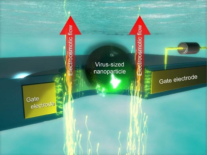
Researchers at Osaka University create voltage-controlled nanopores that can trap particles as they try to pass through, which may lead to single-molecule sensors, along with cheaper and faster genomic sequencing

Credit: Osaka University
Osaka, Japan – Scientists from the Institute of Scientific and Industrial Research at Osaka University fabricated nanopores in silicon dioxide, that were only 300 nm, in diameter surrounded by electrodes. These nanopores could prevent particles from entering just by applying a voltage, which may permit the development of sensors that can detect very small concentrations of target molecules, as well as next-generation DNA sequencing technology.
Nanopores are tiny holes that are wide enough for just a single molecule or particle to pass through. The motion of nanoparticles through these holes can usually be detected as an electrical signal, which makes them a promising platform for novel single-particle sensors. However, control of the motion of the particles has been a challenge so far.
Scientists at Osaka University used integrated nanoelectromechanical systems technology to produce solid-state nanopores, only 300 nm wide, with circular platinum gate electrodes surrounding the openings that can prevent nanoparticles from passing through. This is accomplished by selecting the correct voltage that pulls ions in the solution to create a countervailing flow that blocks the entry of the nanoparticle.
“Single-nanoparticle motions could be controlled via the voltage applied to the surrounding gate electrode, when we fine-tuned the electroosmotic flow via the surface electric potential,” first author Makusu Tsutsui says. After the particle has been trapped at the nanopore opening, a subtle force imbalance between the electrophoretic attraction and the hydrodynamic drag can then be created. At that time, the particles can be pulled in extremely slowly, which may allow long polymers, like DNA, to be threaded through at the correct speed for sequencing.
“The present method can not only enable better sensing accuracy of sub-micrometer objects, such as viruses, but also provides a method for protein structural analysis,” senior author Tomoji Kawai says. While nanopores have already been used to determine the identity of various target molecules based on the current generated, the technology demonstrated in this project may allow for wider range of analytes to be tested this way. For example, small molecules, such as proteins and micro-RNA segments that need to be pulled in at a very controlled speed, may also be detected.
###
The article, “Field effect control of translocation dynamics in surround-gate nanopores,” was published in Communications Materials at DOI: https:/
About Osaka University
Osaka University was founded in 1931 as one of the seven imperial universities of Japan and is now one of Japan’s leading comprehensive universities with a broad disciplinary spectrum. This strength is coupled with a singular drive for innovation that extends throughout the scientific process, from fundamental research to the creation of applied technology with positive economic impacts. Its commitment to innovation has been recognized in Japan and around the world, being named Japan’s most innovative university in 2015 (Reuters 2015 Top 100) and one of the most innovative institutions in the world in 2017 (Innovative Universities and the Nature Index Innovation 2017). Now, Osaka University is leveraging its role as a Designated National University Corporation selected by the Ministry of Education, Culture, Sports, Science and Technology to contribute to innovation for human welfare, sustainable development of society, and social transformation.
Website: https:/
Media Contact
Saori Obayashi
[email protected]
Original Source
https:/
Related Journal Article
http://dx.


