A physics process yielding low-power nanolasers in 2D semiconductor materials could be a game-changer for high speed communications
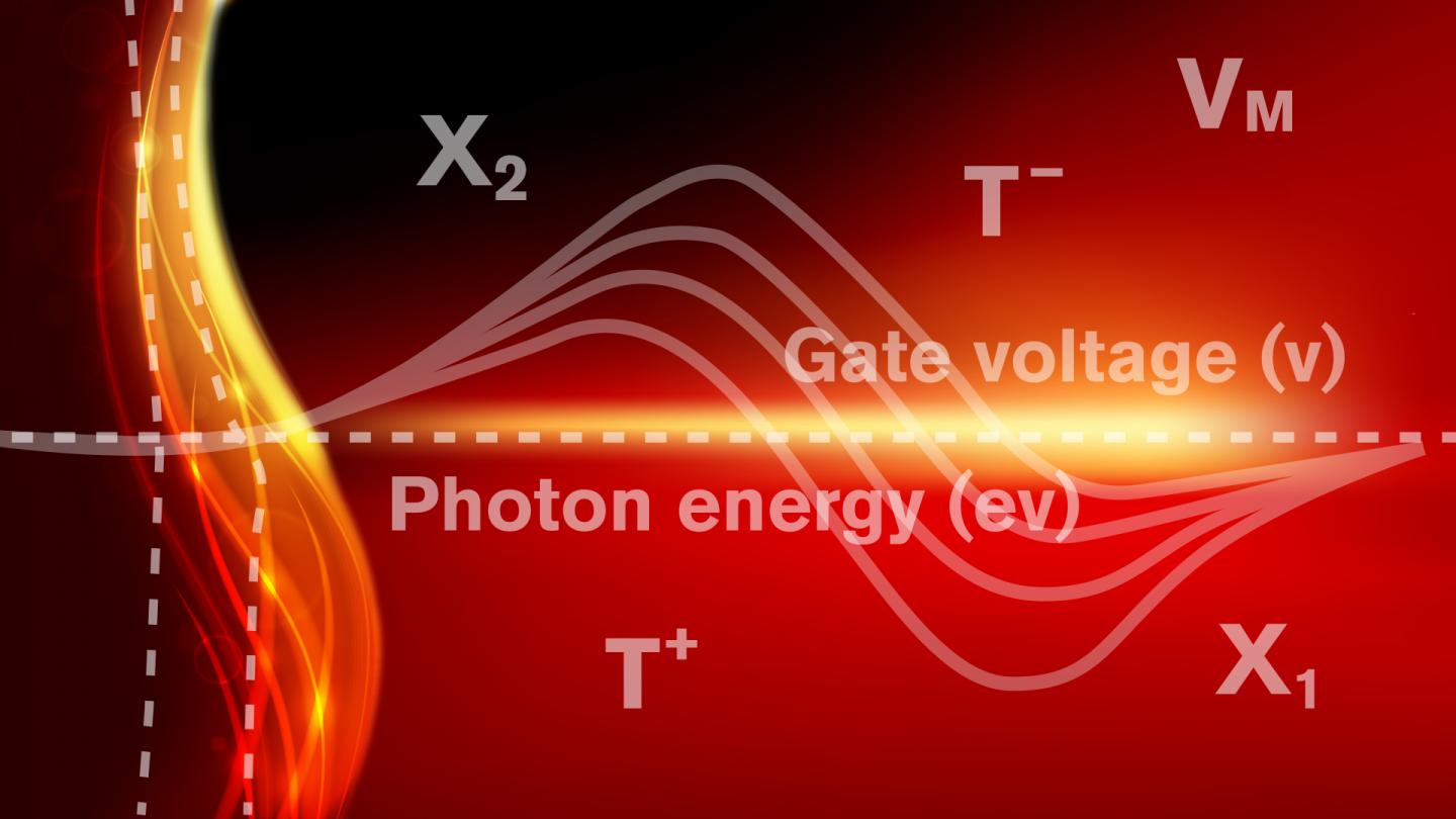
Credit: Graphic by Rhonda Hitchcock-Mast/ASU
In his latest line of research, Cun-Zheng Ning, a professor of electrical engineering in the Ira A. Fulton Schools of Engineering at Arizona State University, and his peers explored the intricate balance of physics that governs how electrons, holes, excitons and trions coexist and mutually convert into each other to produce optical gain. Their results, led by Tsinghua University Associate Professor Hao Sun, were recently published in the Nature publication Light: Science & Applications.
“While studying the fundamental optical processes of how a trion can emit a photon [a particle of light] or absorb a photon, we discovered that optical gain can exist when we have sufficient trion population,” Ning says. “Furthermore, the threshold value for the existence of such optical gain can be arbitrarily small, only limited by our measurement system.”
In Ning’s experiment, the team measured optical gain at density levels four to five orders of magnitude — 10,000 to 100,000 times — smaller than those in conventional semiconductors that power optoelectronic devices, like barcode scanners and lasers used in telecommunications tools.
Ning has been driven to make such a discovery by his interest in a phenomenon called the Mott transition, an unresolved mystery in physics about how excitons form trions and conduct electricity in semiconductor materials to the point that they reach the Mott density (the point at which a semiconductor changes from an insulator to a conductor and optical gain first occurs).
But the electrical power needed to achieve Mott transition and density is far more than what is desirable for the future of efficient computing. Without new low-power nanolaser capabilities like the ones he is researching, Ning says it would take a small power station to operate one supercomputer.
“If optical gain can be achieved with excitonic complexes below the Mott transition, at low levels of power input, future amplifiers and lasers could be made that would require a small amount of driving power,” Ning says.
This development could be game-changing for energy-efficient photonics, or light-based devices, and provide an alternative to conventional semiconductors, which are limited in their ability to create and maintain enough excitons.
As Ning observed in previous experiments with 2D materials, it is possible to achieve optical gain earlier than previously believed. Now he and his team have uncovered a mechanism that could make it work.
“Because of the thinness of the materials, electrons and holes attract each other hundreds of times stronger than in conventional semiconductors,” Ning says. “Such strong charge interactions make excitons and trions very stable even at room temperatures.”
This means the research team could explore the balance of the electrons, holes, excitons and trions as well as control their conversion to achieve optical gain at very low levels of density.
“When more electrons are in the trion state than their original electron state, a condition called population inversion occurs,” Ning says. “More photons can be emitted than absorbed, leading to a process called stimulated emission and optical amplification or gain.”
SOLVING NANOLASER MYSTERIES, ONE STEP OF FUNDAMENTAL SCIENCE AT A TIME
While this new discovery added a piece to the Mott transition puzzle — it uncovered a new mechanism that researchers can exploit to create low-power 2D semiconductor nanolasers — Ning says that they are not yet sure if this is the same mechanism that led to the production of their 2017 nanolasers.
Work is still ongoing in resolving the remaining mysteries.
Similar trion experiments were conducted in the 1990s with conventional semiconductors, Ning says, “but the excitons and trions were so unstable, both experimental observation and, especially, utilization of this optical gain mechanism for real devices are extremely difficult.”
“Since the excitons and trions are much more stable in the 2D materials, there are new opportunities to make real-world devices out of these observations.”
This interesting development by Ning and his research team is only at the fundamental science level. However, fundamental research can lead to exciting things.
“Basic science is a worldwide endeavor and everyone benefits if the best people from everywhere can be involved. ASU has provided an open and free environment, especially for international collaborations with top research groups in China, Germany, Japan and worldwide,” Ning says.
His team has more work left to do to study how this new mechanism of optical gain works at different temperatures — and how to use it to create the nanolasers purposefully.
“The next step is to design lasers that can operate specifically using the new mechanisms of optical gain,” Ning says.
With the physics foundations laid, they could eventually be applied to create new nanolasers that could change the future of supercomputing and data centers.
“The long-term dream is to combine lasers and electronic devices in a single integrated platform, to enable a supercomputer or data center on a chip,” Ning says. “For such future applications, our present semiconductor lasers are still too large to be integrated with electronic devices.”
###
The Ira A. Fulton Schools of Engineering at Arizona State University, with more than 24,000 enrolled students, is the largest engineering school in the United States, offering 46 graduate and 25 undergraduate degree programs across seven schools of academic focus. With students, faculty and researchers representing all 50 states and 135 countries, the Fulton Schools of Engineering is creating an inclusive environment for engineering excellence by advancing research and innovation at scale, revolutionizing engineering education and expanding global outreach and partner engagement. The Fulton Schools of Engineering’s research expenditures totaled $115 million for the 2019-2020 academic year. Learn more about the Fulton Schools of Engineering at engineering.asu.edu.
Media Contact
Lanelle Strawder
[email protected]
Original Source
https:/
Related Journal Article
http://dx.


