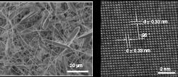
Credit: Sergey Savrasov, UC Davis
Researchers in China and at UC Davis have measured high conductivity in very thin layers of niobium arsenide, a type of material called a Weyl semimetal. The material has about three times the conductivity of copper at room temperature, said Sergey Savrasov, professor of physics at UC Davis. Savrasov is a coauthor on the paper published March 18 in Nature Materials.
New materials that conduct electricity are of great interest to physicists and materials scientists, both for basic research and because they could lead to new types of electronic devices.
Savrasov works on theoretical condensed matter physics. With others, he proposed the existence of Weyl semimetals in 2011. The Chinese team were able to fabricate and test small pieces, called nanobelts, of niobium arsenide, confirming the predictions of theory. The nanobelts are so thin they are essentially two-dimensional.
“A Weyl semimetal is not a conductor or an insulator, but something in between,” Savrasov said. Niobium arsenide, for example, is a poor conductor in bulk but has a metallic surface that conducts electricity. The surface is topologically protected, meaning that it cannot be changed without destroying the bulk material.
With most materials, surfaces can be chemically altered as they pick up impurities from the environment. These impurities can interfere with conductivity. But topologically protected surfaces reject these impurities.
“In theory we expect Weyl surfaces to be good conductors as they don’t tolerate impurities,” Savrasov said.
If you think of electrons flowing through material, imagine them bouncing off or scattering from impurities. At the quantum level, a conductive material has a Fermi surface which describes all the quantum energy states that electrons can occupy. This Fermi surface affects conductivity of the material.
The nanobelts tested in these experiments had a limited Fermi surface or Fermi arc, meaning that electrons could only be scattered to a limited range of quantum states.
“The Fermi arc limits the states electrons can bounce back to, therefore they are not scattered,” Savrasov said.
Materials that are highly conductive at very small scales could be useful as engineers strive to build smaller and smaller circuits. Less electrical resistance means that less heat is generated as current passes through.
###
Coauthors on the paper are Cheng Zhang, Zhuoliang Ni, Jinglei Zhang, Xiang Yuan, Yanwen Liu, Yichao Zou, Zhiming Liao, Yongping Du, Awadhesh Narayan, Hongming Zhang, Tiancheng Gu, Xuesong Zhu, Li Pi, Stefano Sanvito, Xiaodong Han, Jin Zou, and Faxian Xiu. The research institutions represented include Fudan University, Shanghai; Chinese Academy of Sciences, Hefei; Nanjing University of Science and Technology and Nanjing University, Nanjing; Beijing University of Technology; the University of Queensland, Australia; ETH Zurich, Switzerland; and Trinity College Dublin, Ireland. Funding support came from the National Natural Science Foundation of China and other Chinese government agencies; U.S. National Science Foundation; the Australian Research Council; and Science Foundation Ireland.
Media Contact
Andy Fell
[email protected]
Original Source
https:/


