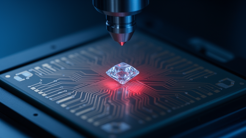
Quantum photonic chips promise to carry the future of quantum computing and quantum communication on structures no larger than a fingernail, yet the field has long been trapped by an awkward materials mismatch. The crystals that host the finest quantum emitters are rarely the crystals from which engineers can build large, low-loss optical circuits. Diamond, the undisputed champion for solid-state quantum emitters and long-lived spin systems, is notoriously difficult to pattern into the sprawling waveguide networks that integrated photonics demands. A research collaboration spanning the United States and the Republic of Korea now reports a way to marry these two worlds without paying the usual penalty in optical loss, and the result may reshape how quantum photonic hardware is built.
Writing in the journal Light: Science & Applications, the team describes a self-aligned heterogeneous photonic integration method that fuses diamond nanobeams containing quantum emitters with titanium dioxide photonic circuits. The published work, titled Self-Aligned Heterogeneous Quantum Photonic Integration, demonstrates not merely a fabrication trick but a functioning platform: a hybrid optical cavity that boosts light emission from a silicon-vacancy center in diamond, on-chip routing of photons emitted by that center, and initialization and readout of the emitter’s spin state directly through the chip. Together, these demonstrations establish that quantum light can be generated, controlled, and collected within a single integrated architecture.
The central insight behind the method is elegantly simple. Rather than trying to place a tiny diamond structure onto a photonic chip with painstaking external alignment, the researchers guide a diamond nanobeam into a pre-patterned structure where it naturally settles into its correct position. The surrounding photonic device is then fabricated around it. Because alignment is built directly into the fabrication process itself, the approach sidesteps the positioning errors and excess insertion losses that have plagued earlier attempts at heterogeneous quantum photonics. The technique transforms what was once a delicate manual assembly problem into a self-correcting manufacturing step.
“We wanted a practical way to combine high-quality quantum emitters with integrated photonics without paying a large price in optical loss,” said Kinfung Ngan, the first author of the study and a graduate student at JILA and the University of Colorado Boulder. That practical motivation runs through every element of the design. Insertion loss, the fraction of light sacrificed whenever a photon crosses from one optical element into another, is the silent killer of quantum photonic scalability. In quantum systems, every lost photon is an irreplaceable quantum resource, and cascaded losses across many interfaces can render even a sophisticated chip useless for real quantum applications.
The choice of materials reflects a careful balancing act. Diamond hosts some of the most celebrated quantum emitters in solid-state physics, including the silicon-vacancy center used in this work, whose spin states can be initialized, manipulated, and read out with high fidelity. Titanium dioxide, by contrast, is a superb material for low-loss photonic circuits and is compatible with mature fabrication processes. Previous efforts to combine them typically relied on active alignment under microscopes or on transfer techniques that left the two materials imperfectly registered, introducing scattering and reflection at every junction. The self-aligned scheme eliminates that fragile step by letting physics do the positioning.
The demonstrated device functions read like a checklist for quantum photonic technology. The hybrid optical cavity formed around the diamond nanobeam enhances the emission rate of the silicon-vacancy center, a phenomenon rooted in cavity quantum electrodynamics that allows a quantum emitter to funnel its photons preferentially into a well-defined optical mode. Once generated, those photons are routed through the titanium dioxide circuit, showing that the interface between the two materials transmits light efficiently enough to preserve the fragile quantum information it carries. Finally, the team showed that the spin state of the emitter could be initialized and read out through the chip, confirming that the full quantum control loop survives integration.
“By showing enhanced emission, on-chip spin control, and efficient photon routing in the same platform, this work points to a realistic path toward scalable quantum photonic chips,” said Dongyeon Daniel Kang, a corresponding author of the study and a senior research scientist at the Korean Institute of Science and Technology. The significance of combining all three functions on a single device cannot be overstated. Many laboratories have demonstrated individual pieces of this puzzle, such as enhanced emission in one architecture or spin control in another, but assembling them within one coherent, low-loss platform has remained the field’s stubborn bottleneck.
The architecture also leaves room for growth. According to the authors, the same platform is compatible with advanced photonic designs for efficient and broadband photon collection, providing a flexible foundation upon which larger and more complex quantum photonic circuits can be erected. Equally important, the self-aligned integration method is not restricted to diamond and titanium dioxide. The researchers emphasize that the approach could extend to other quantum emitters and photonic materials, opening the door to a general integration strategy rather than a bespoke solution for one material pair. That generality could prove decisive as the community explores alternative color centers, defects, and host crystals with their own advantages.
The broader implications reach into the infrastructure of future quantum technologies. Quantum networks will require quantum repeaters, devices that catch, store, and retransmit entangled photons across continental distances, and those repeaters depend on interfaces that marry long-lived spin memories with efficient optical collection. Large-scale photonic quantum processors, meanwhile, will demand thousands of emitters and routing elements stitched together with minimal loss. “By overcoming a key integration bottleneck, this work opens exciting opportunities for large-scale photonic quantum processors and quantum repeaters,” said Shuo Sun, the corresponding author, a JILA Fellow, and an assistant professor at the University of Colorado Boulder.
What makes this advance resonate beyond the laboratory is its framing as a practical route rather than a proof of principle. By reducing optical loss at the material interface and demonstrating generation, control, and collection of quantum light on chip, the work addresses the central question that has shadowed quantum photonics for years: how to connect the best quantum materials to chip-scale photonic technology in a way that survives the transition from a handful of devices to the vast circuits that quantum computers and networks will require. If the self-aligned philosophy proves as extensible as its creators suggest, the marriage of diamond and titanium dioxide may be remembered as the moment integrated quantum photonics acquired its manufacturing playbook.
Subject of Research: Self-aligned heterogeneous integration of diamond quantum emitters with titanium dioxide photonic circuits for low-loss quantum photonic chips
Article Title: A practical route to low-loss integrated quantum photonic chips
Article References: A practical route to low-loss integrated quantum photonic chips. (n.d.). Original publication
Image Credits: AI Generated
DOI: Not provided
Keywords: quantum photonics, diamond nanobeams, silicon-vacancy center, titanium dioxide, heterogeneous integration, insertion loss, spin control, optical cavity, quantum repeaters, integrated photonics, photon routing, quantum networks
News Source: Katie Riggs. (October 18, 2026). Self-aligned diamond chips bring quantum emitters onto photonic circuits with minimal light loss. Scienmag.