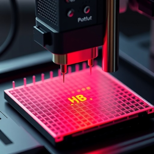
A groundbreaking advancement in nano-printing technology has emerged from South Korea, promising to revolutionize the way ultra-fine metal circuits are transferred onto complex and sensitive surfaces. Traditionally, transferring nanoscale metal patterns onto substrates such as biological tissues or intricately curved surfaces has faced significant obstacles, including the need for high heat, pressure, adhesives, or toxic chemicals. Now, a team of researchers led by distinguished scientists from KAIST and collaborating institutions has unveiled an innovative technique called Water-Floating Nano-Transfer Printing (WF-nTP), enabling the direct transfer of delicate metal circuits onto diverse three-dimensional surfaces without damage or harsh processing conditions.
This cutting-edge technology leverages the simple yet elegant principle of floating ultra-thin metal films on the surface of water. By engineering metal circuits that are as thin as 20 nanometers, composed of materials like gold, platinum, palladium, or nickel, the team managed to float these films on water and then seamlessly transfer them onto curved and irregular surfaces, including living plant leaves, fruits, automotive parts, and the exteriors of robots. Such delicate substrates have long posed formidable challenges to conventional nano-transfer processes which relied heavily on thermal or mechanical input.
Water-Floating Nano-Transfer Printing begins with depositing metal layers onto a specially designed polymer mold. The subsequent step utilizes plasma gas etching, a high-energy ionized gas process, to selectively remove parts of the mold, thereby freeing the nano-metal film. When placed in water, the microscopic gaps within the structure allow water to seep in, delicately releasing the thin metal film so it gently floats atop the water’s surface while maintaining its precise nano-patterned shape. This self-floating film acts like a flexible, near-invisible stamp, perfectly poised for transfer.
The actual transfer to the target surface employs a “scooping” method. The object to be printed on is submerged under the floating metal film, then slowly raised through the water surface, capturing the film onto its exterior. As the water evaporates, capillary forces draw the metal film ever closer to the substrate, and final adhesion is secured by molecular interactions rather than adhesives or external pressure. This ensures the circuit conforms intimately to the target’s surface topology while preserving its structural and functional integrity.
One of the remarkable achievements of this method lies in its compatibility with hydrophobic materials, such as lotus leaves, which typically repel water and have posed significant hurdles for electronic printing methods. By adjusting the surface tension of water through the addition of small amounts of ethanol, the researchers adeptly overcame this repellency barrier, allowing circuits to adhere uniformly even on surfaces designed to shed moisture. This breakthrough opens doors to integrating bioelectronics directly onto natural living organisms and other water-resistant materials.
The versatility and gentleness of WF-nTP technology make it highly promising for groundbreaking applications across multiple fields. The team demonstrated this by fabricating Surface-Enhanced Raman Scattering (SERS) sensors and transferring them onto leaf and fruit surfaces. These sensors allow for highly sensitive detection of trace chemical substances, exemplified by the successful identification of thiram, a pesticide residue, directly on plants. Such capability paves the way for smart agricultural systems that monitor crop health and contamination without causing harm.
Moreover, the researchers exhibited the method’s applicability in wearable health monitoring by creating flexible hydrogen gas sensors. By transferring palladium mesh structures onto thermoplastic polyurethane (TPU) fibers—materials known for their elasticity and comfort—they developed ultrathin, flexible sensors suitable for integration into wearable devices. This could herald new eras of unobtrusive, high-performance bioelectronic devices capable of continuous health monitoring and environmental sensing.
Distinguished Professor Inkyu Park emphasized the profound implications of this innovation, noting that WF-nTP obliterates the substrate limitations typical of existing nano-transfer printing technologies. The capacity to faithfully transfer nano-patterns onto living tissues, human skin, or complex three-dimensional objects without heat or adhesives presages transformative impacts in wearable electronics, bioelectronics, electronic skins for robotics, and precision agriculture. Such a versatile platform technology stands poised to underpin the next generation of sensor-integrated systems embedded into everyday objects and organisms.
The interdisciplinary collaboration spanned multiple institutions, combining expertise in mechanical engineering, materials science, and applied physics. Alongside Professor Park, key contributors included Dr. Jun-Ho Jeong from the Korea Institute of Machinery and Materials and Professor Junseong Ahn from Korea University, supported by a dedicated team of researchers. PhD candidate Byung-Ho Kang led the experimental investigations, authoring the principal study that documents these technological advancements.
Published in the prestigious journal Nature Communications on March 30, 2026, this research outlines both the conceptual framework and experimental realizations of Water-Floating Nano-Transfer Printing. The paper extensively details the fabrication processes, plasma etching techniques, physics of film flotation, and adhesion mechanics. The publication has stirred considerable interest within the scientific community due to its potential to reshape nano-manufacturing paradigms.
Financially backed by South Korea’s Ministry of Science and ICT through the National Research Foundation and the Ministry of Trade, Industry and Energy via the Korea Evaluation Institute of Industrial Technology (KEIT) Alchemist Project, this work benefits from robust institutional support. Such investment underscores the national strategic priority on advancing nano-scale electronics and flexible device technologies as drivers of future industrial innovation.
Crucially, WF-nTP exemplifies a leap toward sustainable nano-fabrication by eliminating the need for harsh chemicals, elevated temperatures, or external adhesives, thus reducing environmental footprint and enabling integration with living organisms without injury or toxicity. As the boundaries between electronics and biology continue to blur, technologies like this pave the way for seamless interfaces between the digital and biological worlds.
From smart agricultural sensors monitoring pesticide residues in real-time to wearable biosensors tracking human health metrics effortlessly, Water-Floating Nano-Transfer Printing ushers in an era of flexible, ultra-thin, and conformal electronics. This breakthrough holds immense promise for advancing personalized medicine, environmental monitoring, robotic sensing, and beyond—transforming how we interact with and augment living and non-living surfaces at the nanoscale.
Subject of Research:
Nano-transfer printing technology for transferring ultra-thin metal circuits onto diverse 3D and sensitive surfaces, including biological tissue, curved automotive parts, and wearable fibers.
Article Title:
Water-Floating Nano-Transfer Printing Enables Damage-Free Circuit Integration on Complex and Living Surfaces
News Publication Date:
30-Mar-2026
Web References:
http://dx.doi.org/10.1038/s41467-026-70902-5
Image Credits:
KAIST
Keywords:
Water-Floating Nano-Transfer Printing, WF-nTP, nano-circuits, flexible electronics, bioelectronics, wearable sensors, surface-enhanced Raman scattering, hydrophobic surfaces, plasma etching, capillary adhesion, palladium mesh sensors, pesticide detection, smart agriculture
Tags: delicate metal circuits on 3D surfacesflexible electronics manufacturinginnovative nano-transfer techniquesKAIST nano-technology researchlow-temperature nano-fabricationmetal nano-films on curved surfacesnano-printing technology advancementnano-transfer printing on biological tissuesnanoscale metal pattern transfernon-toxic nano-transfer methodsultra-fine metal circuit transferWater-Floating Nano-Transfer Printing

