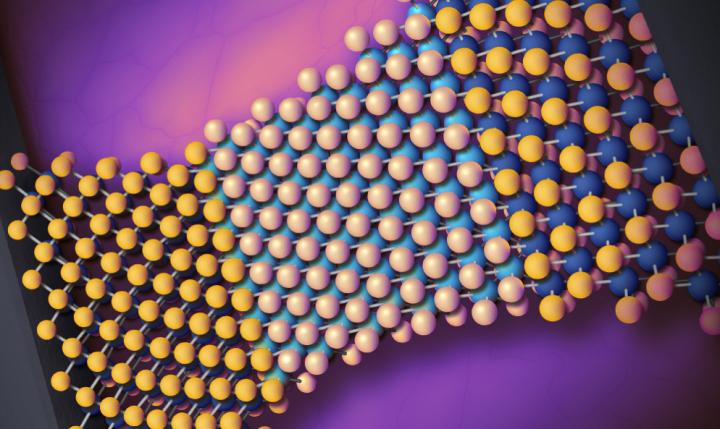
Credit: University of Rochester illustration / Michael Osadciw
Two-dimensional (2D) materials – as thin as a single layer of atoms – have intrigued scientists with their flexibility, elasticity, and unique electronic properties, as first discovered in materials such as graphene in 2004. Some of these materials can be especially susceptible to changes in their material properties as they are stretched and pulled. Under applied strain, they have been predicted to undergo phase transitions as disparate as superconducting in one moment to nonconducting the next, or optically opaque in one moment to transparent in the next.
Now, University of Rochester researchers have combined 2D materials with oxide materials in a new way, using a transistor-scale device platform, to fully explore the capabilities of these changeable 2D materials to transform electronics, optics, computing and a host of other technologies.
“We’re opening up a new direction of study,” says Stephen Wu, assistant professor of electrical and computer engineering and physics. “There’s a huge number of 2D materials with different properties – and if you stretch them, they will do all sorts of things.”
The platform developed in Wu’s lab, configured much like traditional transistors, allows a small flake of a 2D material to be deposited onto a ferroelectric material. Voltage applied to the ferroelectric — which acts like a transistor’s third terminal, or gate -strains the 2D material by the piezoelectric effect, causing it to stretch. That, in turn, triggers a phase change that can completely change the way the material behaves. When the voltage is turned off the material retains its phase until an opposite polarity voltage is applied, causing the material to revert to its original phase.
“The ultimate goal of two-dimensional straintronics is to take all of the things that you couldn’t control before, like the topological, superconducting, magnetic, and optical properties of these materials, and now be able to control them, just by stretching the material on a chip,” Wu says.
“If you do this with topological materials you could impact quantum computers, or if you do it with superconducting materials you can impact superconducting electronics.”
In a paper in Nature Nanotechnology, Wu and his students describe using a thin film of two-dimensional molybdenum ditelluride (MoTe2) in the device platform. When stretched and unstretched, the MoTe2 changes from a low conductivity semiconductor material to a highly conductive semimetallic material and back again.
“It operates just like a field effect transistor. You just have to put a voltage on that third terminal, and the MoTe2 will stretch a little bit in one direction and become something that’s conducting. Then you stretch it back in another direction, and all of a sudden you have something that has low conductivity,” Wu says.
The process works at room temperature, he adds, and, remarkably, “requires only a small amount of strain – we’re stretching the MoTe2 by only 0.4 percent to see these changes.”
Moore’s law famously predicts that the number of transistors in a dense integrated circuit doubles about every two years.
However, as technology nears the limits at which traditional transistors can be scaled down in size — as we reach the end of Moore’s law — the technology developed in Wu’s lab could have far-reaching implications in moving past these limitations as the quest for ever more powerful, faster computing continues.
Wu’s platform has the potential to perform the same functions as a transistor with far less power consumption since power is not needed to retain the conductivity state. Moreover, it minimizes the leakage of electrical current due to the steep slope at which the device changes conductivity with applied gate voltage. Both of these issues — high power consumption and leakage of electrical current — have constrained the performance of traditional transistors at the nanoscale.
“This is the first demonstration,” Wu adds. “Now it’s up to researchers to figure out how far it goes.”
One advantage of Wu’s platform is that it is configured much like a traditional transistor, making it easier to eventually adapt into current electronics. However, more work is needed before the platform reaches that stage. Currently the device can operate only 70 to 100 times in the lab before device failure. While the endurance of other non-volatile memories, like flash, are much higher they also operate much slower than the ultimate potential of the strain-based devices being developed in Wu’s lab.
“Do I think it’s a challenge that can be overcome? Absolutely,” says Wu, who will be working on the problem with Hesam Askari, an assistant professor of mechanical engineering at Rochester, also a co-author on the paper. “It’s a materials engineering problem that we can solve as we move forward in our understanding how this concept works.”
They will also explore how much strain can be applied to various two-dimensional materials without causing them to break. Determining the ultimate limit of the concept will help guide researchers to other phase-change materials as the technology moves forward
Wu, who completed his PhD in physics at the University of California, Berkeley, was a postdoctoral scholar in the Materials Science Division at Argonne National Laboratory before he joined the University of Rochester as an assistant professor in the Department of Electrical and Computer Engineering and the Department of Physics in 2017.
He started with a single undergraduate student in his lab — Arfan Sewaket ’19, who was spending the summer as a Xerox Research Fellow. She helped Wu set up a temporary lab, then was the first to try out the device concept and the first to demonstrate its feasibility.
Since then, four graduate students in Wu’s lab — lead author Wenhui Hou, Ahmad Azizimanesh, Tara Pen?a, and Carla Watson “have done so much work” to document the device’s properties and refine it, creating about 200 different versions to this point, Wu says. All are listed with Sewaket as coauthors, along with Askari and Ming Liu of Xi’an Jiaotong University in China.
###
Media Contact
Bob Marcotte
[email protected]
Related Journal Article
http://dx.

