Researchers solve decades-old challenge of building a functional transistor integrated with ferroelectric RAM
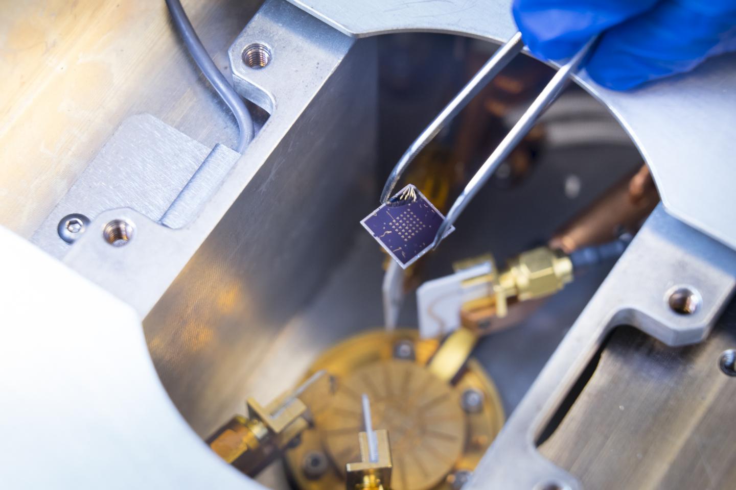
Credit: Purdue University photo/Vincent Walter
WEST LAFAYETTE, Ind. — A computer chip processes and stores information using two different devices. If engineers could combine these devices into one or put them next to each other, then there would be more space on a chip, making it faster and more powerful.
Purdue University engineers have developed a way that the millions of tiny switches used to process information – called transistors – could also store that information as one device.
The method, detailed in a paper published in Nature Electronics, accomplishes this by solving another problem: combining a transistor with higher-performing memory technology than is used in most computers, called ferroelectric RAM.
Researchers have been trying for decades to integrate the two, but issues happen at the interface between a ferroelectric material and silicon, the semiconductor material that makes up transistors. Instead, ferroelectric RAM operates as a separate unit on-chip, limiting its potential to make computing much more efficient.
A team led by Peide Ye, the Richard J. and Mary Jo Schwartz Professor of Electrical and Computer Engineering at Purdue, discovered how to overcome the mortal enemy relationship between silicon and a ferroelectric material.
“We used a semiconductor that has ferroelectric properties. This way two materials become one material, and you don’t have to worry about the interface issues,” Ye said.
The result is a so-called ferroelectric semiconductor field-effect transistor, built in the same way as transistors currently used on computer chips.
The material, alpha indium selenide, not only has ferroelectric properties, but also addresses the issue of a conventional ferroelectric material usually acting as an insulator rather than a semiconductor due to a so-called wide “band gap,” which means that electricity cannot pass through and no computing happens.
Alpha indium selenide has a much smaller band gap, making it possible for the material to be a semiconductor without losing ferroelectric properties.
Mengwei Si, a Purdue postdoctoral researcher in electrical and computer engineering, built and tested the transistor, finding that its performance was comparable to existing ferroelectric field-effect transistors, and could exceed them with more optimization. Sumeet Gupta, a Purdue assistant professor of electrical and computer engineering, and Ph.D. candidate Atanu Saha provided modeling support.
Si and Ye’s team also worked with researchers at the Georgia Institute of Technology to build alpha indium selenide into a space on a chip, called a ferroelectric tunneling junction, which engineers could use to enhance a chip’s capabilities. The team presents this work on Dec. 9 at the 2019 IEEE International Electron Devices Meeting.
In the past, researchers hadn’t been able to build a high-performance ferroelectric tunneling junction because its wide band gap made the material too thick for electrical current to pass through. Since alpha indium selenide has a much smaller band gap, the material can be just 10 nanometers thick, allowing more current to flow through it.
More current allows a device area to scale down to several nanometers, making chips more dense and energy efficient, Ye said. A thinner material – even down to an atomic layer thick – also means that the electrodes on either side of a tunneling junction can be much smaller, which would be useful for building circuits that mimic networks in the human brain.
###
This research was performed in the Purdue Discovery Park Birck Nanotechnology Center and supported by the National Science Foundation, Air Force Office of Scientific Research, Semiconductor Research Corporation, Defense Advanced Research Projects Agency and the U.S. Office of Naval Research.
About Discovery Park
Discovery Park is a place where Purdue researchers move beyond traditional boundaries, collaborating across disciplines and with policymakers and business leaders to create solutions for a better world. Grand challenges of global health, global conflict and security, and those that lie at the nexus of sustainable energy, world food supply, water and the environment are the focus of researchers in Discovery Park. The translation of discovery to impact is integrated into the fabric of Discovery Park through entrepreneurship programs and partnerships.
ABSTRACTS
A Ferroelectric Semiconductor Field-Effect Transistor
Mengwei Si, Atanu K. Saha, Shengjie Gao, Gang Qiu, Jingkai Qin, Yuqin Duan, Jie Jian, Chang Niu, Haiyan Wang, Wenzhuo Wu, Sumeet K. Gupta, Peide D. Ye
Purdue University, West Lafayette, IN, USA
DOI: 10.1038/s41928-019-0338-7
A ferroelectric semiconductor field-effect transistor (FeS-FET) was proposed and experimentally demonstrated. In this novel FeS-FET, a two-dimensional (2D) ferroelectric semiconductor α-In2Se3 is used to replace conventional semiconductor as channel. α-In2Se3 is identified due to its proper bandgap, room temperature ferroelectricity, the ability to maintain ferroelectricity down to a few atomic layers and the feasibility for large-area growth. An atomic-layer deposition (ALD) Al2O3 passivation method was developed to protect and enhance the performance of the α-In2Se3 FeS-FETs. The fabricated FeS-FETs exhibit high performance with a large memory window, a high on/off ratio over 108, a maximum on-current of 862 μA/μm, low supply voltage with scaled gate insulator and the potential to exceed the existing Fe-FETs for non-volatile memory applications.
A Novel Scalable Energy-Efficient Synaptic Device: Crossbar Ferroelectric Semiconductor Junction
Si1, Y. Luo2, W. Chung1, H. Bae1, D. Zheng1, J. Li1, J. Qin1, G. Qiu1, S. Yu2, and P. D. Ye1
1 Purdue University, West Lafayette, IN, USA
2 Georgia Institute of Technology, Atlanta, GA, USA
A novel ferroelectric semiconductor junction (FSJ) based two-terminal memristor is demonstrated as a synaptic device for the first time. In this novel FSJ device, a metal-ferroelectric semiconductor (FS)-metal crossbar structure is used, instead of a metal-ferroelectric insulator-metal structure for a conventional ferroelectric tunnel junction (FTJ), so that an ultra-thin ferroelectric insulator is not required. Meanwhile, the FSJ also offers energy efficiency advantage over the conventional filament-based resistive random access memory (RRAM) device because the conductance of the FSJ scales with the junction area. Experimentally, a ferroelectric semiconductor α-In2Se3 based crossbar FSJ (c-FSJ) as a synaptic device is demonstrated. Ferroelectric resistive switching is clearly observed in both planar FSJ (p-FSJ) by in-plane polarization switching and c-FSJ by out-of-plane polarization switching. Conductance potentiation and depression in the c-FSJ are measured and benchmarked at both original size and projected to 32 nm node with different synaptic devices. α-In2Se3 c-FSJ shows good on-line learning accuracy (~92 %), low latency and energy consumption due to the short write pulse width and large RON.
Media Contact
Kayla Wiles
[email protected]
765-494-2432
Original Source
https:/
Related Journal Article
http://dx.


