


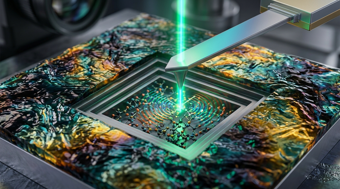
Scientists have developed a practical way to predict how easily amorphous chalcogenide thin films can be carved away at the nanoscale, using nothing more exotic than Raman spectroscopy and a diamond-coated atomic force microscopy probe. The work, published in Applied Microscopy, addresses a stubborn problem in the study of materials destined for phase-change memory and threshold-switching devices: without knowing how resistant a film is to tip-induced wear, researchers cannot reliably perform the layer-by-layer etching that three-dimensional tomographic imaging demands.
The research team, led by Siwon Park, Young-Min Kim and Jong-Souk Yeo, focused on amorphous chalcogenides such as Ge-Te, Si-Te and Ge-Se, materials whose fast-switching behavior underpins emerging memory technologies. Confirming and characterizing these electrical changes requires three-dimensional tomographic imaging capable of resolving structural and compositional changes across a film. Atomic force microscopy is well suited to this task because it can alternate etching and imaging steps, and it also enables both electrical measurement and biasing during etching, which is essential given the volatile nature of Ovonic Threshold Switching behavior. Yet accurate AFM-based etching demands a quantitative understanding of tip-induced wear resistance, and amorphous materials, lacking long-range structural order, make that resistance difficult to predict from local bonding configurations and surface-mediated contact mechanics alone.
To build that understanding, the team deposited binary amorphous chalcogenide thin films of Ge22-Te78, Si58-Te42 and Ge77-Se23 on silicon dioxide substrates by RF co-sputtering, each roughly 50 nanometers thick, and confirmed their compositions by X-ray photoelectron spectroscopy. Etching was performed in contact mode over a 5 by 5 micrometer squared area, and the resulting morphology and depth were examined in non-contact mode over a larger 10 by 10 micrometer squared confirming region. Both steps used a diamond-coated conductive probe with a nominal tip radius of about 100 to 200 nanometers and a nominal spring constant near 80 newtons per meter. A fresh probe was used for each film, and all experiments on a given film shared the same probe.
The researchers systematically increased the load from 1200 to 2200 nanonewtons in 200-nanonewton increments, repeating each load three times at previously uncontacted locations to avoid cumulative damage. After each etching scan, the same probe reimaged the area in non-contact mode to measure the etched morphology and depth. Force-distance pull-off measurements, taken on unetched areas before and after the 18 etching scans, tracked the probe state throughout. The pull-off force decreased by 16 percent for Ge-Te, 13 percent for Si-Te and 26 percent for Ge-Se relative to pre-etch values, indicating a change in the probe state in which wear or damage of the coating and surface contamination could not be separated. For all three films, the mean etched depth increased with increasing load.
To interpret these measurements, the team combined the Archard sliding wear law with the Derjaguin-Muller-Toporov contact model, chosen because the measured pull-off forces were finite but small, roughly 3 to 11 percent of the applied loads, so adhesion could be treated as an additional force acting outside the contact area. This analysis yielded a composite wear parameter, denoted Wr, that merges the wear coefficient and the effective hardness into a single quantity, allowing relative comparison of the films under identical nanoscale AFM contact conditions. Fitting the load-depth data separately in a low-load range of 1200 to 1600 nanonewtons and a high-load range of 1800 to 2200 nanonewtons, the researchers found the same ordering in both ranges: Ge-Te showed the largest Wr, followed by Si-Te, then Ge-Se. The values, expressed in units of 10⁻¹⁰ square meters per newton, were 3.63, 1.91 and 0.86 in the low-load range and 4.94, 3.62 and 1.69 in the high-load range for Ge-Te, Si-Te and Ge-Se respectively, with differences between films exceeding the combined standard uncertainties. Because Wr decreases as hardness increases, the ordering marks Ge-Te as the relatively softest film and Ge-Se as the hardest under these conditions.
The next challenge was explaining this ordering without independent nanoindentation. The team turned to Raman spectroscopy, which revealed the dominant bonding configurations in each film: Te-Te chain vibrations and Ge-Te stretching modes in Ge-Te, Te-Te chains and Si-Te stretching in Si-Te, and Ge-Se bonds, Se-Se intrachain stretching and broadened Ge-Ge bonds in Ge-Se. By weighting standard bond enthalpies, calculated using Pauling’s rule as reported in the Lankhorst model, with the normalized Raman area fractions, the researchers computed an effective bond enthalpy for each film. The resulting values were 223, 333 and 394 kilojoules per mole for GeTe, SiTe and GeSe respectively. This monotonically increasing sequence mirrored the decreasing trend in the composite wear parameter across both load ranges, indicating that films with a weaker average bond network are more sensitive to nanoscale etching. The authors note that because the Raman area reflects scattering cross-sections as well as bond concentrations, the effective bond enthalpy serves as a descriptor for ranking films rather than as an absolute bond enthalpy.
The real test came when the framework was applied beyond the binary systems used to construct it. The team calculated the effective bond enthalpy of an amorphous ternary Si13-Ge07-Te80 film from its Raman spectrum, inserted the value into the linear fit established from the three binary films, and obtained a predicted composite wear parameter of 4.01 times 10⁻¹⁰ square meters per newton. Because this parameter encapsulates both wear coefficient and effective hardness without requiring their independent determination, it directly provided the slope of the etched depth versus applied load curve, assumed to pass through the origin consistent with a measured adhesion force of 185 nanonewtons. Based on this model, a load of 350 nanonewtons was selected to target an etched depth of approximately 5 nanometers per layer.
Etching proceeded by contact-mode scanning over a 2.5 by 2.5 micrometer squared area, repeated for four successive layers, with each etching step followed by non-contact imaging to confirm depth and roughness. Across the four layers, the etched depths were 7.5, 4.0, 4.1 and 1.9 nanometers, giving a mean of 4.4 plus or minus 2.3 nanometers, which falls 12.3 percent below the modeled target of 5 nanometers. Although the mean agrees reasonably well with the model, the inter-layer variability is substantial, and surface roughness increased progressively with etched depth. The researchers attribute the declining depth in later layers to piled-up material accumulating at the edges of the repeatedly etched region: the probe collides with this accumulated material in subsequent steps, reducing etching efficiency, in agreement with the rise of the surface roughness of the etched region from 3.58 to 4.41 nanometers. Because the layers were etched successively at the same position with the same probe, they are not independent replicates, and the team regards the result as a first-pass validation of the load selection rather than an accurate prediction.
The authors also identify two sources of the deviation from the target. First, the relationship between effective bond enthalpy and the wear parameter was built from binary films, and the linear fit assumes the composite parameter scales similarly for ternary compositions, even though the additional element in Si-Ge-Te introduces cross-bonding configurations absent from the binary training set that may shift both the wear coefficient and hardness in ways the single-variable descriptor cannot capture. Second, the wear parameter was determined from loads of 1200 to 2200 nanonewtons, whereas the tomography deliberately ran at a much lower 350 nanonewtons to achieve the shallow depth required for depth-resolved imaging, and extrapolating to this load, together with the assumed adhesion force, introduces uncertainty that partially accounts for the observed discrepancy.
The results are explicitly relative and probe specific. The pull-off force of each probe decreased during etching, the loads are nominal values, and the ternary test was limited to one film with four non-independent layers. Future work, the authors suggest, should include replicate probes with direct probe observation, monitoring of the probe state during etching, and a larger calibration set including additional ternary and quaternary compositions. They also propose reducing pile-up by shrinking the etched region step by step, an approach that remains to be tested. Even with these caveats, the team reports that this represents, to their knowledge, the first use of a compositional bond-enthalpy descriptor to predict the composite wear parameter and thereby guide load selection for nanoscale etching of amorphous chalcogenides across varied compositions, laying groundwork for systematic extension to broader ternary and quaternary systems and offering a non-destructive alternative to nanoindentation for choosing starting etching conditions.
Subject of Research: Raman-guided prediction of nanoscale wear resistance for AFM tomography of amorphous chalcogenide thin films
Article Title: Nanoscale etching characteristics for controlled AFM tomography of amorphous chalcogenide thin films
Article References: Park, S., Kim, Y.-M., & Yeo, J.-S. (2026). Nanoscale etching characteristics for controlled AFM tomography of amorphous chalcogenide thin films. Applied Microscopy, 56(1), Article 27. https://doi.org/10.1186/s42649-026-00147-5
Image Credits: AI Generated
DOI: 10.1186/s42649-026-00147-5
Keywords: atomic force microscopy, amorphous chalcogenides, Raman spectroscopy, phase-change memory, threshold switching, nanoscale etching, wear resistance, bond enthalpy, tomography, thin films, Ge-Te, Si-Ge-Te
News Source: Denise Maddox. (November 3, 2026). Raman-Guided AFM Etching Opens New Window Into Amorphous Chalcogenide Films. Scienmag.