Credit: Evan Simmons and Kun Li
WEST LAFAYETTE, Ind. — Electronics are increasingly being paired with optical systems, such as when accessing the internet on an electronically run computer through fiber optic cables.
But meshing optics — which relies on particles of light called photons–with electronics–relying on electrons — is challenging, due to their disparate scales. Electrons work at a much smaller scale than light does. The mismatch between electronic systems and optical systems means that every time a signal converts from one to the other, inefficiency creeps into the system.
Now, a team led by a Purdue University scientist has found a way to create more efficient metamaterials using semiconductors and a novel aspect of physics that amplifies the activity of electrons. The study is published in the journal Optica.
This new class of materials has the potential to dramatically increase the resolution in medical scanning and scientific imaging and drastically reduce the size of supercomputers, creating a future where scientists can see tiny things in far greater detail and devices are smaller and more powerful.
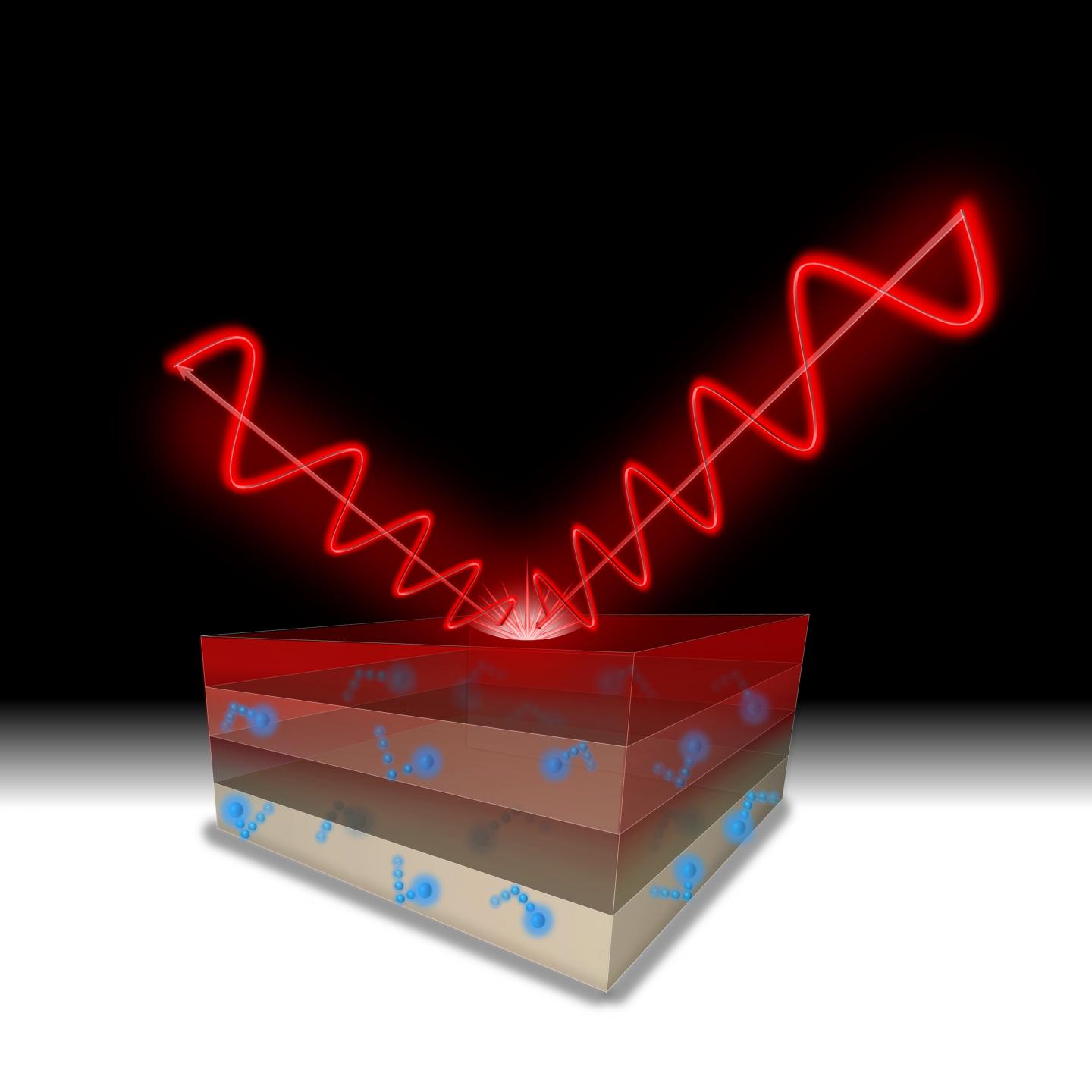
Scientists have worked for decades to shrink photons down to a nanometer scale to make them more compatible with electrons — a field known as nanophononics. This can be achieved using rarefied materials and expensive production techniques to make so-called hyperbolic materials. Using hyperbolic materials, scientists can shrink photons by compressing the light, making it easier to interface with electrical systems.
Evgenii Narimanov, a theoretical physicist and professor of electrical and computer engineering at Purdue, explained, “The most important thing about hyperbolic materials is that they can compress light to almost any scale. When you can make light small, you solve the problem of the disconnect between optics and electronics. Then you can make very efficient optoelectronics.”
The problem lies in creating these hyperbolic materials. They typically consist of interwoven layers of metals and dielectrics, and every surface must be as smooth and defect-free as possible at the atomic level, something that is difficult, time-consuming and expensive.
The solution, Narimanov believes, includes semiconductors. Not, he emphasized, because of anything special about the semiconductors themselves. But because scientists and researchers have devoted the past 70 years or more to producing high-quality semiconductors efficiently. Narimanov wondered if he could harness that proficiency and apply it to producing new and improved metamaterials.
Unfortunately, semiconductors do not make inherently good optical metamaterials; they do not have enough electrons. They can work at relatively low frequencies, in the mid- to far-infrared scale. But to improve imaging and sensing technologies, scientists need metamaterials that work in the visible on near-infrared spectrum, at much shorter wavelengths than the mid- and far-infrared.
Narimanov and his collaborators discovered and tested an optical phenomenon called “ballistic resonance.” In these new optical materials, which combine metamaterial concepts with the atomic precision of single-crystal semiconductors, free (ballistic) electrons interact with an oscillating optical field.
Synchronizing the optical field with the frequency of the motion of the free electrons as they bounce within the confines of the thin conducting layers, forming the composite material, causes the electrons to resonate, enhancing the reaction of each electron and creating a metamaterial that works at higher frequencies. While the researchers were not yet able to reach the wavelengths of the visible spectrum, they did get 60% of the way there.
“We showed that there is a physics mechanism that makes this possible,” Narimanov said. “Before, people did not realize this was something that could be done. We have opened the way. We showed it is theoretically possible, and then we experimentally demonstrated 60% improvement in the operational frequency over existing materials.”
Narimanov originated the idea and then teamed up with Kun Li, Andrew Briggs, Seth Bank and Daniel Wasserman at the University of Texas, as well as Evan Simmons and Viktor Podolskiy at the University of Massachusetts Lowell. The University of Texas researchers developed the fabrication technology, while the Massachusetts Lowell scientists contributed to the full quantum theory and performed the numerical simulations to be sure everything functioned as planned.
“We will keep pushing this frontier,” Narimanov said. “Even if we are extremely successful, nobody is going to get semiconductor metamaterials to the visible and near-infrared spectrum within a year or two. It may take about five years. But what we have done is provide the material platform. The bottleneck for photonics is in the material where electrons and photons can meet on the same length scale, and we have solved it.”
###
This work was partially supported by the National Science Foundation (grants DMR-1629276, DMR-1629330, DMR-1629570 and ECCS-1926187), the Defense Advanced Research Projects Agency Nascent Light-Matter Interactions program, and the Gordon and Betty Moore Foundation.
ABSTRACT
Ballistic Metamaterials
Kun Lia, Evan Simmons, A. F. Briggs, S. R. Banka, Daniel Wasserman, Viktor A. Podolskiy, Evgenii E. Narimanov
DOI: 10.1364/OPTICA.402891
We report the theoretical prediction and experimental realization of a new optical phenomenon, ballistic resonance. This resonance, resulting from the interplay between free charge motion in confining geometries and periodic driving electromagnetic fields, can be utilized to achieve negative permittivity at frequencies well above the bulk plasma frequency. The ballistic resonance, therefore, enables the realization and deployment of various applications that rely on local field enhancement and emission modulation, typically associated with plasmonic materials, in new materials platforms. As a proof of principle, we demonstrate all-semiconductor hyperbolic metamaterials operating at frequencies 60% above the plasma frequency of the constituent doped semiconductor “metallic” layer.
Media Contact
Kayla Wiles
[email protected]
Original Source
https:/
Related Journal Article
http://dx.


