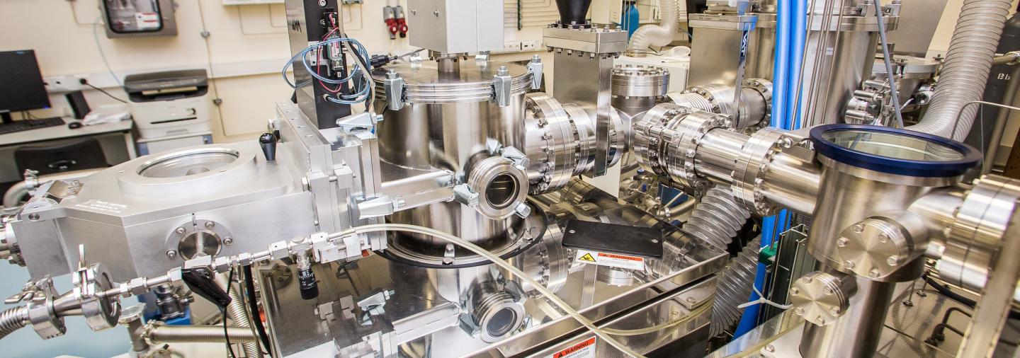
Credit: Atomic Layer Deposition Lab, MIPT
Researchers from the Moscow Institute of Physics and Technology have managed to grow atomically thin films of molybdenum disulfide spanning up to several tens of square centimeters. It was demonstrated that the material’s structure can be modified by varying the synthesis temperature. The films, which are of interest to electronics and optoelectronics, were obtained at 900-1,000 degrees Celsius. The findings were published in the journal ACS Applied Nano Materials.
Two-dimensional materials are attracting considerable interest due to their unique properties stemming from their structure and quantum mechanical restrictions. The family of 2D materials includes metals, semimetals, semiconductors, and insulators. Graphene, which is perhaps the most famous 2D material, is a monolayer of carbon atoms. It has the highest charge-carrier mobility recorded to date. However, graphene has no band gap under standard conditions, and that limits its applications.
Unlike graphene, the optimal width of the bandgap in molybdenum disulfide (MoS2) makes it suitable for use in electronic devices. Each MoS2 layer has a sandwich structure, with a layer of molybdenum squeezed between two layers of sulfur atoms. Two-dimensional van der Waals heterostructures, which combine different 2D materials, show great promise as well. In fact, they are already widely used in energy-related applications and catalysis. Wafer-scale (large-area) synthesis of 2D molybdenum disulfide shows the potential for breakthrough advances in the creation of transparent and flexible electronic devices, optical communication for next-generation computers, as well as in other fields of electronics and optoelectronics.
“The method we came up with to synthesize MoS2 involves two steps. First, a film of MoO3 is grown using the atomic layer deposition technique, which offers precise atomic layer thickness and allows conformal coating of all surfaces. And MoO3 can easily be obtained on wafers of up to 300 millimeters in diameter. Next, the film is heat-treated in sulfur vapor. As a result, the oxygen atoms in MoO3 are replaced by sulfur atoms, and MoS2 is formed. We have already learned to grow atomically thin MoS2 films on an area of up to several tens of square centimeters,” explains Andrey Markeev, the head of MIPT’s Atomic Layer Deposition Lab.
The researchers determined that the structure of the film depends on the sulfurization temperature. The films sulfurized at 500 ? contain crystalline grains, a few nanometers each, embedded in an amorphous matrix. At 700 ?, these crystallites are about 10-20 nm across and the S-Mo-S layers are oriented perpendicular to the surface. As a result, the surface has numerous dangling bonds. Such structure demonstrates high catalytic activity in many reactions, including the hydrogen evolution reaction. For MoS2 to be used in electronics, the S-Mo-S layers have to be parallel to the surface, which is achieved at sulfurization temperatures of 900-1,000 ?. The resulting films are as thin as 1.3 nm, or two molecular layers, and have a commercially significant (i.e., large enough) area.
The MoS2 films synthesized under optimal conditions were introduced into metal-dielectric-semiconductor prototype structures, which are based on ferroelectric hafnium oxide and model a field-effect transistor. The MoS2 film in these structures served as a semiconductor channel. Its conductivity was controlled by switching the polarization direction of the ferroelectric layer. When in contact with MoS2, the La:(HfO2-ZrO2) material, which was earlier developed in the MIPT lab, was found to have a residual polarization of approximately 18 microcoulombs per square centimeter. With a switching endurance of 5 million cycles, it topped the previous world record of 100,000 cycles for silicon channels.
###
The research team acknowledges the financial support of the Russian Science Foundation (Project No. 19-19-00504).
The Atomic Layer Deposition Lab conducts research into all the key aspects of modern atomic layer deposition methods. The main research goal is the development of new functional materials for the semiconductor industry, including nonvolatile memory devices. In particular, the lab’s researchers created a novel thin-film ferroelectric material with a switching endurance of 100 billion cycles with titanium nitride electrodes. In contrast, flash memory can withstand no more than 100,000 write-erase cycles. Another area of interest is the development of biocompatible coatings, including those with tailored electrical properties. The researchers came up with a crystalline modification of titanium oxide that has good biocompatibility with bone tissue. They also suggested a new technology and process for coating titanium dental implants, reducing the time it takes for an implant to settle down from about three months to just two weeks.
Media Contact
Ilyana Zolotareva
[email protected]
897-777-14699
Original Source
https:/
Related Journal Article
http://dx.


