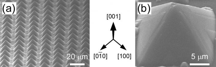
Researchers from Nara Institute of Science and Technology fabricated arrays of atomically smooth iron-coated silicon pyramids, with unusual magnetic properties
Credit: Ken Hattori
Ikoma, Japan – Ultrasmall integrated circuits have revolutionized mobile phones, home appliances, cars, and other everyday technologies. To further miniaturize electronics and enable advanced functions, circuits must be reliably fabricated in three dimensions. Achieving ultrafine 3D shape control by etching into silicon is difficult because even atomic-scale damage reduces device performance. Researchers at Nara Institute of Science and Technology (NAIST) report, in a new study seen in Crystal Growth and Design, silicon etched to adopt the shape of atomically smooth pyramids. Coating these silicon pyramids with a thin layer of iron imparts magnetic properties that until now were only theoretical.
NAIST researcher and senior author of the study Ken Hattori is widely published in the field of atomically controlled nanotechnology. One focus of Hattori’s research is in improving the functionality of silicon-based technology.
“Silicon is the workhorse of modern electronics because it can act as a semiconductor or an insulator, and it’s an abundant element. However, future technological advances require atomically smooth device fabrication in three dimensions,” says Hattori.
A combination of standard dry etching and chemical etching is necessary to fabricate arrays of pyramid-shaped silicon nanostructures. Until now, atomically smooth surfaces have been extremely challenging to prepare.
“Our ordered array of isosceles silicon pyramids were all the same size and had flat facet planes. We confirmed these findings by low-energy electron diffraction patterns and electron microscopy,” explains lead author of the study Aydar Irmikimov.
An ultrathin – 30 nanometer – layer of iron was deposited onto the silicon to impart unusual magnetic properties. The pyramids’ atomic-level orientation defined the orientation-and thus the properties-of the overlaying iron.
“Epitaxial growth of iron enabled shape anisotropy of the nanofilm. The curve for the magnetization as a function of the magnetic field was rectangular-like shaped but with breaking points which were caused by asymmetric motion of magnetic vortex bound in pyramid apex,” explains Hattori.
The researchers found that the curve had no breaking points in analogous experiments performed on planar iron-coated silicon. Other researchers have theoretically predicted the anomalous curve for pyramid shapes, but the NAIST researchers are the first to have shown it in a real nanostructure.
“Our technology will enable fabrication of a circular magnetic array simply by tuning the shape of the substrate,” says Irmikimov. Integration into advanced technologies such as spintronics – which encode information by the spin, rather than electrical charge, of an electron – will considerably accelerate the functionality of 3D electronics.
###
Resource
Title: Atomically architected silicon pyramid single-crystalline structure supporting epitaxial material growth and characteristic magnetism
Authors: Aydar Irmikimov, Liliany N. Pamasi, Azusa N. Hattori, Takaaki Higashi, Shunta Takahashi, Emilia E. Hashamova, Xiaoqian Shi, Fangzhun Guo, Nobuyoshi Hosoito, Ai I. Osaka, Hidekazu Tanaka & Ken Hattori
Journal: Crystal Growth and Design
DOI: 10.1021/acs.cgd.0c01286
Information about the Surface and Materials Physics Laboratory at NAIST can be found at the following website:
https:/
Media Contact
Takahito Shikano
[email protected]
Related Journal Article
http://dx.


