


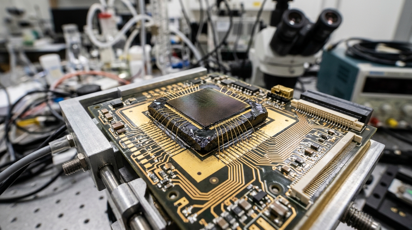
A numerical modeling study demonstrates that pursuing exceptionally high sensitivity in direct semiconductor X-ray detectors is unnecessary for substantially lowering radiation exposure, revealing that an eighty percent medical dose reduction requires detector sensitivity only on the order of 103 μCGy−1⋅cm−2. Researchers showed that achieving high detective quantum efficiency depends critically on balancing detector sensitivity with circuit-level saturation limits, dark current suppression, and spatial pixel uniformity rather than optimizing sensitivity in isolation.
Flat-panel X-ray detectors serve essential roles in medical imaging and non-destructive industrial testing, where diagnostic image quality is evaluated through the detective quantum efficiency metric. This efficiency value is determined by a detector’s intrinsic sensitivity, spatial resolution, and response uniformity across its imaging area.
Commercial markets are currently dominated by indirect flat-panel detectors that rely on scintillators such as thallium-doped cesium iodide. Most indirect commercial detectors demonstrate detective quantum efficiency values below 0.7 because optical crosstalk and multi-step conversion from X-rays to visible light and subsequently to electrical charges restrict overall sensitivity below 103 μCGy−1air⋅cm−2. Direct semiconductor detectors, including amorphous selenium, cadmium telluride, and metal halide perovskites, convert X-ray photons directly into electron-hole pairs in a single step, yielding theoretically superior spatial resolution, higher sensitivity, and higher detective quantum efficiency.
Perovskite-based direct X-ray detectors have demonstrated sensitivities exceeding 104 μCGy−1air⋅cm−2 alongside low detection limits, positioning them as promising candidates for next-generation radiation imaging systems. Prior research concentrated primarily on enhancing material composition and crystal quality to elevate sensitivity and detection thresholds. However, translating these materials into functional flat-panel systems requires integration with front-end pixel readout circuits, such as thin-film transistor arrays, where system-level interactions governing detective quantum efficiency have remained largely unaddressed.
To establish a systematic framework guiding device integration, the researchers formulated a device-level decomposition of detective quantum efficiency grounded in the International Electrotechnical Commission standard IEC-62220-1. The foundational standard defines detective quantum efficiency as a function of spatial frequency, conversion gain, modulation transfer function, and the ratio of input noise power spectrum to output noise power spectrum.
In the derived mathematical model, conversion gain represents the number of electrons generated per incident X-ray photon, which corresponds directly to X-ray sensitivity divided by elementary charge and spectral X-ray photon fluence. For the standard RQA5 spectrum utilized in general radiography, the photon fluence is specified at 30,174 photons per square millimeter per microgray. Input noise power spectrum incorporates pixel area to match the area-independent output noise power spectrum expressed in electrons, which is calculated as the quadratic sum of distinct device and electronic noise components.
The quantitative model incorporates operational constraints imposed by front-end electronic readout circuitry, establishing that the combined signal generated by dark current, X-ray absorption, and electronic noise must not exceed the circuit’s full-well charge capacity. By evaluating zero-frequency imaging conditions where the modulation transfer function equals unity, the authors derived an analytical relationship directly connecting zero-frequency detective quantum efficiency to detector sensitivity, dark current density, frame rate, pixel area, and full-well capacity.
The sensor features a pixel pitch of 75 micrometers by 75 micrometers and a rated exposure dose of 2.5 microgray for general diagnostic radiography.
Applying the model to an imaging scenario operating at one-fifth of the rated exposure dose, or 0.5 microgray, revealed a maximum compatible sensitivity boundary of 8,942.5 μCGy−1air⋅cm−2, compared to 233.5 μCGy−1air⋅cm−2 at full rated dose, beyond which induced charges oversaturate readout capacitors. Analysis of dose-dependent single-pixel noise against total image noise indicated that background noise originates predominantly from pixel-to-pixel non-uniformity rather than temporal readout fluctuations, demonstrating that lower detector sensitivity requires lower spatial variance to achieve high efficiency.
Numerical simulations evaluating the trade-offs between dark current density, sensitivity, and noise under maximum-well conditions established that detective quantum efficiency decreases as dark current density increases. Achieving a high detective quantum efficiency of 0.7 at one-fifth normal medical dose requires sensitivity between 1,248 and 8,171 μCGy−1air⋅cm−2 when dark current density is controlled between 10 and 100 nanoamperes per square centimeter, accompanied by pixel signal variations constrained between 7,610 and 18,612 electrons, corresponding to current density fluctuations between 0.21 and 1.37 nanoamperes per square centimeter.
Addressing the disconnect in detector development, prior investigations into direct semiconductor X-ray detectors concentrated almost exclusively on optimizing crystal growth and adjusting chemical compositions to maximize sensitivity and lower detection limits. However, these device-level improvements were pursued largely in isolation from the operational requirements of thin-film transistor arrays and integrated pixel readout circuits. Previous theoretical formulations of detective quantum efficiency rarely incorporated direct semiconductor mechanisms, leaving researchers without a quantitative roadmap to guide direct flat-panel engineering. By bridging device physics and electronic circuit constraints, the analytical model resolves this gap, demonstrating how fundamental material properties govern the overall detective quantum efficiency of complete imaging systems.
In formulating the relationship between detective quantum efficiency and physical detector metrics, the framework establishes a precise normalization between incoming radiation and electronic noise. The input noise power spectrum depends directly on radiation dose, spectral photon fluence, and pixel area. Because the output noise power spectrum is quantified strictly in units of electrons, it remains inherently independent of physical pixel dimensions. Multiplying the input spectrum by pixel area reconciles this dimensional disparity, enabling an exact comparison between incident X-ray photon statistics and the total output noise. The total electronic noise represents the quadratic sum of all distinct device and circuit noise contributions, defining the overall amplitude of system perturbations.
The operational boundaries of flat-panel detectors are tightly governed by the charge collection limits of front-end electronic capacitors. Within each pixel circuit, the cumulative charge encompasses dark current generation, X-ray absorption, and associated electronic noise, all of which must remain within the maximum full-well capacity. The dark charge accumulation scales proportionally with dark current density and pixel area, while being inversely proportional to the imaging frame rate. When sensors operate at slower frame rates or elevated dark currents, baseline leakage consumes an excessive portion of the full-well capacity. Consequently, the remaining charge capacity available for recording diagnostic X-ray signals shrinks, which severely impairs zero-frequency detective quantum efficiency even before signal processing begins.
To isolate the primary sources of image degradation, the researchers analyzed single-pixel electrical noise as a linear function of incident radiation dose and readout circuit noise. In this formulation, single-pixel noise variance equals the product of radiation dose and dose-dependent conversion gain, combined with the intrinsic noise of the readout circuit. In experimental evaluations of the Dexela 2923 sensor, the measured conversion gain reached 285,372 electrons per microgray of air, corresponding to an effective X-ray sensitivity of 811.7 μCGy−1air⋅cm−2. Because this measured sensitivity falls well below the maximum compatible sensitivity limit calculated for general radiography, the sensor avoids charge saturation while maintaining stable readout performance under standard operating conditions.
A critical observation from the noise analysis is the stark contrast between individual pixel temporal fluctuations and total image noise across the full sensor array. The dose-dependent electrical noise generated within a single pixel proved to be substantially lower than the overall system noise measured across multiple pixels. This disparity indicates that image degradation in flat-panel systems stems predominantly from spatial pixel-to-pixel response variations rather than temporal fluctuations occurring within individual pixels over time. Even highly sensitive direct conversion layers cannot achieve high detective quantum efficiency if subtle material irregularities create spatial response disparities across neighboring pixels.
The numerical simulations further illuminated the direct competitive trade-off between dark current density and usable X-ray sensitivity under maximum-well operating assumptions. Under conditions where dark current signals and X-ray-induced charges collectively saturate pixel storage capacitors, any increase in dark current density directly suppresses the maximum sensitivity that a detector can support. Furthermore, the maximum detective quantum efficiency achievable by the detector decreases continuously as dark current density rises. When dark current density hovers near 10−8 A⋅cm−2, the operational ceiling for detector sensitivity becomes tightly constrained. Lowering dark current from 100 down to 10 nA⋅cm−2 expands the accessible sensitivity window, but doing so simultaneously imposes stricter tolerances on permissible pixel-to-pixel current fluctuations.
These quantitative findings provide a definitive framework that redirects perovskite X-ray detector development away from one-dimensional sensitivity gains and toward balanced device-circuit integration. Instead of engineering materials solely to exceed sensitivities of 104 μCGy−1air⋅cm−2, the model demonstrates that matching moderate sensitivities around 103 μCGy−1air⋅cm−2 with low dark current density and rigorous pixel uniformity is sufficient to achieve superior imaging quality at one-fifth the typical medical exposure dose. The research team emphasizes that this modeling methodology offers practical diagnostic guidance for tailoring perovskite active layers to commercial readout architectures. According to the published report, the datasets supporting the quantitative modeling and sensor calculations remain available from the corresponding author upon reasonable request.
Subject of Research: Quantitative modeling and operational requirements of perovskite direct X-ray flat panel detectors
Article Title: Quantitative modeling of perovskite-based direct X-ray flat panel detectors
Article References: Song, Z., Wang, G., Pang, J., Zheng, Z., Xu, L., Zhou, Y., Niu, G., & Tang, J. (2024). Quantitative modeling of perovskite-based direct X-ray flat panel detectors. Frontiers of Optoelectronics, 17(1), Article 32. https://doi.org/10.1007/s12200-024-00136-0
Image Credits: AI Generated
DOI: 10.1007/s12200-024-00136-0
Keywords: perovskite detectors, direct X-ray detection, detective quantum efficiency, flat-panel detectors, radiation dose reduction, dark current density, numerical modeling, Quantitative, modeling, perovskite-based, direct, X-ray
News Source: Denise Maddox. (November 9, 2026). Numerical Model Sets Target Parameters for Perovskite Direct X-Ray Detectors. Scienmag.