• HOME
  • NEWS
  • EXPLORE
    • CAREER
      • Companies
      • Jobs
    • EVENTS
    • iGEM
      • News
      • Team
    • PHOTOS
    • VIDEO
    • WIKI
  • BLOG
  • COMMUNITY
    • FACEBOOK
    • INSTAGRAM
    • TWITTER
Friday, September 12, 2025
BIOENGINEER.ORG
No Result
View All Result
  • Login
  • HOME
  • NEWS
  • EXPLORE
    • CAREER
      • Companies
      • Jobs
        • Lecturer
        • PhD Studentship
        • Postdoc
        • Research Assistant
    • EVENTS
    • iGEM
      • News
      • Team
    • PHOTOS
    • VIDEO
    • WIKI
  • BLOG
  • COMMUNITY
    • FACEBOOK
    • INSTAGRAM
    • TWITTER
No Result
View All Result
Bioengineer.org
No Result
View All Result
Home NEWS Science News

New way to control electrical charge in 2D materials: Put a flake on it

Bioengineer by Bioengineer
January 14, 2021
in Science News
Reading Time: 2 mins read
0
IMAGE
Share on FacebookShare on TwitterShare on LinkedinShare on RedditShare on Telegram

IMAGE

Credit: (Image courtesy Nano Letters)

Physicists at Washington University in St. Louis have discovered how to locally add electrical charge to an atomically thin graphene device by layering flakes of another thin material, alpha-RuCl3, on top of it.

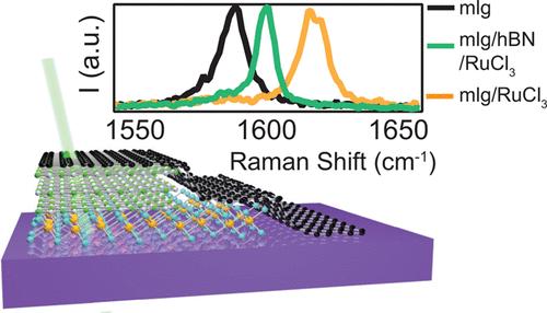
A paper published in the journal Nano Letters describes the charge transfer process in detail. Gaining control of the flow of electrical current through atomically thin materials is important to potential future applications in photovoltaics or computing.

“In my field, where we study van der Waals heterostructures made by custom-stacking atomically thin materials together, we typically control charge by applying electric fields to the devices,” said Erik Henriksen, assistant professor of physics in Arts & Sciences and corresponding author of the new study, along with Ken Burch at Boston College. “But here it now appears we can just add layers of RuCl33. It soaks up a fixed amount of electrons, allowing us to make ‘permanent’ charge transfers that don’t require the external electric field.”

Jesse Balgley, a graduate student in Henriksen’s laboratory at Washington University, is second author of the study. Li Yang, professor of physics, and his graduate student Xiaobo Lu, also both at Washington University, helped with computational work and calculations, and are also co-authors.

Physicists who study condensed matter are intrigued by alpha-RuCl3 because they would like to exploit certain of its antiferromagnetic properties for quantum spin liquids.

In this new study, the scientists report that alpha-RuCl3 is able to transfer charge to several different types of materials — not just graphene, Henriksen’s personal favorite.

They also found that they only needed to place a single layer of alpha-RuCl3 on top of their devices to create and transfer charge. The process still works, even if the scientists slip a thin sheet of an electrically insulating material between the RuCl3 and the graphene.

“We can control how much charge flows in by varying the thickness of the insulator,” Henriksen said. “Also, we are able to physically and spatially separate the source of charge from where it goes — this is called modulation doping.”

Adding charge to a quantum spin liquid is one mechanism thought to underlie the physics of high-temperature superconductivity.

“Anytime you do this, it could get exciting,” Henriksen said. “And usually you have to add atoms to bulk materials, which causes lots of disorder. But here, the charge flows right in, no need to change the chemical structure, so it’s a ‘clean’ way to add charge.”

###

Read more in Nano Letters: Modulation Doping via a Two-Dimensional Atomic Crystalline Acceptor

Media Contact
Talia Ogliore
[email protected]

Original Source

https://source.wustl.edu/2021/01/new-way-to-control-electrical-charge-in-2d-materials-put-a-flake-on-it/

Related Journal Article

http://dx.doi.org/10.1021/acs.nanolett.0c03493

Tags: Chemistry/Physics/Materials SciencesElectrical Engineering/ElectronicsMaterialsSuperconductors/SemiconductorsTechnology/Engineering/Computer Science
Share12Tweet8Share2ShareShareShare2

Related Posts

blank

Auranofin’s Anti-Leishmanial Effects: Lab and Animal Studies

September 12, 2025

Nanomedicine: A New Frontier in Targeting Metastasis

September 12, 2025

Fungal Effector Undermines Maize Immunity by Targeting ZmLecRK1

September 12, 2025

New Phthalide Compounds Show Promise as Antifungal Agents

September 12, 2025
Please login to join discussion

POPULAR NEWS

  • blank

    Breakthrough in Computer Hardware Advances Solves Complex Optimization Challenges

    152 shares
    Share 61 Tweet 38
  • New Drug Formulation Transforms Intravenous Treatments into Rapid Injections

    116 shares
    Share 46 Tweet 29
  • Physicists Develop Visible Time Crystal for the First Time

    64 shares
    Share 26 Tweet 16
  • A Laser-Free Alternative to LASIK: Exploring New Vision Correction Methods

    49 shares
    Share 20 Tweet 12

About

We bring you the latest biotechnology news from best research centers and universities around the world. Check our website.

Follow us

Recent News

Auranofin’s Anti-Leishmanial Effects: Lab and Animal Studies

Nanomedicine: A New Frontier in Targeting Metastasis

Fungal Effector Undermines Maize Immunity by Targeting ZmLecRK1

  • Contact Us

Bioengineer.org © Copyright 2023 All Rights Reserved.

Welcome Back!

Login to your account below

Forgotten Password?

Retrieve your password

Please enter your username or email address to reset your password.

Log In
No Result
View All Result
  • Homepages
    • Home Page 1
    • Home Page 2
  • News
  • National
  • Business
  • Health
  • Lifestyle
  • Science

Bioengineer.org © Copyright 2023 All Rights Reserved.