A research team, led by Professor Kyoung-Duck Park in the Department of Physics at UNIST has succeeded in investigating and controlling the physical properties of naturally-formed nanoscale wrinkles in two-dimensional (2D) semiconductors. This is thanks to their previously-developed hyperspectral adaptive tip-enhanced photoluminescence (a-TEPL) spectroscopy. This will be a major step forward in developing paper-thin, ultra-flexible displays.
Wrinkles are an inevitable structural deformation in 2D semiconductor materials, which gives rise to spatial heterogeneity in material properties, according to the research team. Such structural deformation has long been considered one of the top technical challenges in semiconductor manufacturing, as this would harm the uniformity in structural, electrical, and optical properties of semiconductors. Besides, because the size of these wrinkles is quite small, the accurate analysis of their structural, optical, and excitonic properties has been impossible with conventional spectroscopic tools. “Recent strain-engineering approaches have enabled to tune of some of these properties, yet there has been no attempt to control the induced strain of naturally-formed nanoscale wrinkles, while simultaneously investigating their modified nano-optical properties,” noted the research team.
In this study, the research team presented a hyperspectral TEPL nano-imaging approach, combined with nano-optomechanical strain control, to investigate and control the nano-optical and -excitonic properties of naturally-formed wrinkles in a WSe2 ML. This approach allowed them to reveal the modified electronic properties and exciton behaviors at the wrinkle, associated with the induced uniaxial tensile strain at the apex. Based on this, the research team was able to exploit the wrinkle structure as a nanoscale strain-engineering platform. The precise atomic force tip control also enabled them to engineer the excitonic properties of TMD MLs at the nano-local regions in a fully reversible fashion, noted the research team.
The research team further presented a more systematic platform for dynamic nano-emission control of the wrinkle by demonstrating programmably-operational switching and modulation modes in time and space. “We envision that our approach gives access to potential applications in quantum-nanophotonic devices, such as bright nano-optical sources for light-emitting diodes, nano-optical switch/multiplexer for optical integrated circuits, and exciton condensate devices,” said the research team.
Meanwhile, Professor Ki Kang Kim and Dr. Soo Ho Choi from Sungkyunkwan University, and Professor Hyun Seok Lee from Chungbuk National University participated in the production of 2D semiconductor materials used in the study. Professor Geunsik Lee and Dr. Yongchul Kim from the Department of Chemistry at UNIST also participated in the theoretical calculation of the findings.
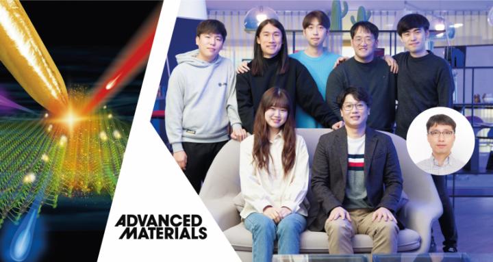
The findings of this research have been published in the online version of Advanced Materials, ahead of print, on May 11, 2021. It has also been selected as the front cover of the April 2021 issue of the journal. Besides, the source technology of this nano-mechanical strain-engineering was granted an official patent.
###
Media Contact
JooHyeon Heo
[email protected]
Original Source
https:/


