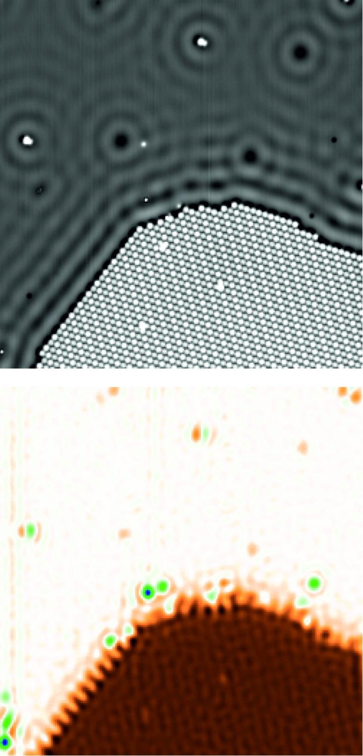
Credit: Copyright: Forschungszentrum Jülich / Christian Wagner
A team of researchers from Jülich in cooperation with the University of Magdeburg has developed a new method to measure the electric potentials of a sample at atomic accuracy. Using conventional methods, it was virtually impossible until now to quantitatively record the electric potentials that occur in the immediate vicinity of individual molecules or atoms. The new scanning quantum dot microscopy method, which was recently presented in the journal Nature Materials by scientists from Forschungszentrum Jülich together with partners from two other institutions, could open up new opportunities for chip manufacture or the characterization of biomolecules such as DNA.
The positive atomic nuclei and negative electrons of which all matter consists produce electric potential fields that superpose and compensate each other, even over very short distances. Conventional methods do not permit quantitative measurements of these small-area fields, which are responsible for many material properties and functions on the nanoscale. Almost all established methods capable of imaging such potentials are based on the measurement of forces that are caused by electric charges. Yet these forces are difficult to distinguish from other forces that occur on the nanoscale, which prevents quantitative measurements.
Four years ago, however, scientists from Forschungszentrum Jülich discovered a method based on a completely different principle. Scanning quantum dot microscopy involves attaching a single organic molecule – the “quantum dot” – to the tip of an atomic force microscope. This molecule then serves as a probe. “The molecule is so small that we can attach individual electrons from the tip of the atomic force microscope to the molecule in a controlled manner,” explains Dr. Christian Wagner, head of the Controlled Mechanical Manipulation of Molecules group at Jülich’s Peter Grünberg Institute (PGI-3).
The researchers immediately recognized how promising the method was and filed a patent application. However, practical application was still a long way off. “Initially, it was simply a surprising effect that was limited in its applicability. That has all changed now. Not only can we visualize the electric fields of individual atoms and molecules, we can also quantify them precisely,” explains Wagner. “This was confirmed by a comparison with theoretical calculations conducted by our collaborators from Luxembourg. In addition, we can image large areas of a sample and thus show a variety of nanostructures at once. And we only need one hour for a detailed image.”
The Jülich researchers spent years investigating the method and finally developed a coherent theory. The reason for the very sharp images is an effect that permits the microscope tip to remain at a relatively large distance from the sample, roughly 2-3 nanometres – unimaginable for a normal atomic force microscope.
In this context, it is important to know that all elements of a sample generate electric fields that influences the quantum dot and can therefore be measured. The microscope tip acts as a protective shield that dampens the disruptive fields from areas of the sample that are further away. “The influence of the shielded electric fields thus decreases exponentially, and the quantum dot only detects the immediate surrounding area,” explains Wagner. “Our resolution is thus much sharper than could be expected from even an ideal point probe.”
The Jülich researchers owe the speed at which the complete sample surface can be measured to their partners from Otto von Guericke University Magdeburg. Engineers there developed a controller that helped to automate the complex, repeated sequence of scanning the sample. “An atomic force microscope works a bit like a record player,” says Wagner. “The tip moves across the sample and pieces together a complete image of the surface. In previous scanning quantum dot microscopy work, however, we had to move to an individual site on the sample, measure a spectrum, move to the next site, measure another spectrum, and so on, in order to combine these measurements into a single image. With the Magdeburg engineers’ controller, we can now simply scan the whole surface, just like using a normal atomic force microscope. While it used to take us 5-6 hours for a single molecule, we can now image sample areas with hundreds of molecules in just one hour.”
There are some disadvantages as well, however. Preparing the measurements takes a lot of time and effort. The molecule serving as the quantum dot for the measurement has to be attached to the tip beforehand – and this is only possible in a vacuum at low temperatures. In contrast, normal atomic force microscopes also work at room temperature, with no need for a vacuum or complicated preparations.
And yet, Prof. Stefan Tautz, director at PGI-3, is optimistic: “This does not have to limit our options. Our method is still new, and we are excited for the first projects so we can show what it can really do.”
There are many fields of application for quantum dot microscopy. Semiconductor electronics is pushing scale boundaries in areas where a single atom can make a difference for functionality. Electrostatic interaction also plays an important role in other functional materials, such as catalysts. The characterization of biomolecules is another avenue. Thanks to the comparatively large distance between the tip and the sample, the method is also suitable for rough surfaces – such as the surface of DNA molecules, with their characteristic 3D structure.
###
Media Contact
Tobias Schlößer
[email protected]
Original Source
https:/
Related Journal Article
http://dx.


