The rapid advancement of artificial intelligence (AI) continues to revolutionize various sectors, extending beyond the tech industry and permeating healthcare, finance, manufacturing, and even education. As these innovations surge forward, one critical aspect driving this transformation is the need for enhanced computational power. Conventional AI frameworks primarily rely on graphical processing units (GPUs) for model training. However, GPUs come with significant challenges, particularly concerning processing efficiency and energy consumption. The quest for a robust and sustainable infrastructure for AI has led researchers to explore alternative solutions that promise improvements in both performance and energy efficiency.
A groundbreaking study published in the IEEE Journal of Selected Topics in Quantum Electronics has introduced a novel AI acceleration platform that utilizes photonic integrated circuits (PICs). This approach promises superior scalability and energy efficiency, significantly outpacing traditional GPU-based architectures. Spearheaded by Dr. Bassem Tossoun, a Senior Research Scientist at Hewlett Packard Labs, this research underscores the potential of PICs to revolutionize the way AI workloads are executed. The integration of III-V compound semiconductors within these circuits allows for remarkable operational efficiency, setting the stage for a new era of AI hardware.
Photonic AI accelerators introduce optical neural networks (ONNs), which operate at the speed of light, drastically reducing energy loss compared to conventional electronic distributed neural networks (DNNs). This shift from electronic to optical processing represents a substantial leap in the processing capabilities of AI systems, aligning with the demands of increasingly complex AI applications. Dr. Tossoun highlighted this transition, pointing out the inherent advantages offered by silicon photonics, which while easy to manufacture, have historically posed challenges for scaling complex integrated circuits.
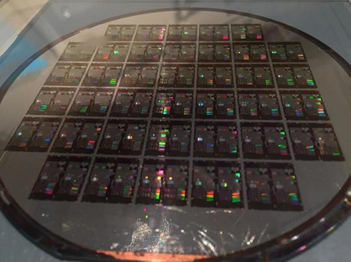
The innovative approach employed by Tossoun and his team involved a heterogeneous integration of silicon photonics along with III-V compound semiconductors. This fusion of technologies enhances the infrastructure’s capacity to integrate essential components—such as lasers and optical amplifiers—thereby minimizing optical losses and improving overall system scalability. Such advancements enable PICs to house numerous functionalities in a compact footprint, making them ideal candidates for next-generation AI accelerators.
Dr. Tossoun remarked, “The heterogeneous III/V-on-SOI platform presents the foundational components essential for advancing photonic and optoelectronic computing architectures tailored for AI/ML acceleration.” These architectures are highly relevant for analog machine learning photonic accelerators that utilize continuous analog values, diverging significantly from conventional digital approaches that tend to exacerbate energy inefficiencies.
By achieving wafer-scale integration, the photonic platform enables the construction of optical neural networks on a single chip, incorporating vital components such as on-chip lasers, amplifiers, photodetectors, modulators, and phase shifters. This extensive integration contributes to a dramatic increase in energy efficiency, with the new platform reportedly achieving a footprint-energy efficiency that is 2.9 × 10² times greater than previous photonic systems and 1.4 × 10² times more efficient than the most sophisticated digital electronics available today.
This revolution in AI technology, specifically through the lens of photonic circuits, hints at transformative potential across various applications. Addressing energy costs and computational challenges will empower data centers to handle an influx of AI workloads, ultimately leading to enhanced capabilities in solving complex optimization problems—a necessity in today’s data-driven landscape. The future implications of this research stretch far and wide, indicating a shift towards a more sustainable, efficient, and high-performance computational paradigm for AI applications.
The emergence of these photonic integrated circuits heralds a new chapter in AI hardware that is not merely an enhancement but a complete redefinition of what is possible in machine learning and artificial intelligence. As these technological advancements reach maturation, industries can anticipate a significant transformation in their operational capabilities, leading to more resilient and sophisticated AI-driven solutions.
The promise of PICs extends beyond mere efficiency; it encapsulates a vision of a future where AI computations can occur with minimal resource expenditure while maximizing performance outputs. This newly developed platform paves the way for robust, energy-efficient AI hardware, ensuring that technological progression remains both sustainable and responsible in an ever-evolving digital landscape.
As researchers and engineers continue to refine these photonic approaches, the boundaries between algorithmic abilities and hardware limitations will increasingly diminish. This synergy will not only enhance AI’s current applications but will also unlock entirely new possibilities—enabling machines to learn and adapt at unprecedented rates, fundamentally transforming our relationship with technology.
In summary, the work done by Tossoun and his team represents a paradigm shift in how technological advancements can align with the future energy and computational needs of AI. This innovation is imperative for fostering a thriving environment for AI development, where efficiency meets scalability and performance, laying the groundwork for a new generation of intelligent systems.
Subject of Research: Photonic integrated circuits for AI acceleration
Article Title: Large-Scale Integrated Photonic Device Platform for Energy-Efficient AI/ML Accelerators
News Publication Date: 9-Jan-2025
Web References: IEEE Journal of Selected Topics in Quantum Electronics
References: Tossoun, B., et al. (2025). Large-Scale Integrated Photonic Device Platform for Energy-Efficient AI/ML Accelerators. IEEE Journal of Selected Topics in Quantum Electronics.
Image Credits: Bassem Tossoun from IEEE JSTQE
Keywords
Tags: advancements in AI computational poweralternatives to GPU for AIDr. Bassem Tossoun’s research contributionsenergy-efficient AI computingIEEE research on AI hardwareIII-V compound semiconductors in photonicsoptical neural networks technologyphotonic integrated circuits in AIrevolutionizing AI with photonicsscalable AI acceleration platformssilicon photonics for AI hardwaresustainable AI infrastructure

