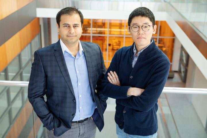
Credit: Photo by L. Brian Stauffer
CHAMPAIGN, Ill. — A University of Illinois-based team of engineers has found that the model currently used to predict heat loss in a common semiconductor material does not apply in all situations. By testing the thermal properties of gallium nitride semiconductors fabricated using four popular methods, the team discovered that some techniques produce materials that perform better than others. This new understanding can help chip manufacturers find ways to better diffuse the heat that leads to device damage and decreased device lifespans.
Silicon chips are being pushed to their limit to meet the demands of today’s electronic devices. Gallium nitride, another semiconductor material, is better suited for use in high-voltage and high-current applications like those needed for 5G phones, “internet of things” devices, robotics and autonomous vehicles. Gallium nitride chips are already in use, but there are no systematic studies that examine the thermal properties of the various forms of the material, the researchers said. Their findings are published in the Journal of Applied Physics.
Gallium nitride chips are produced by depositing gallium nitride vapor onto a surface where it crystallizes into a solid, the researchers said.
“The composition and atomic structure of the surface used to grow the crystals influences the number of defects in the final product,” said Can Bayram, an electrical and computer engineering professor and lead author of the study. “For example, crystals grown on silicon surfaces produce a semiconductor with many defects – resulting in lower thermal conductivity and hotter hotspots – because the atomic structures of silicon and gallium nitride are very different.”
The team tested the thermal conductivity of gallium nitride grown using the four most technologically important fabrication techniques: hydride vapor phase epitaxy, high nitride pressure, vapor deposition on sapphire and vapor deposition on silicon.
To figure out how the different fabrication techniques influence the thermal properties of gallium nitride, the team measured thermal conductivity, defect density and the concentration of impurities of each material.
“Using our new data, we were able to develop a model that describes how defects affect the thermal properties of gallium nitride semiconductors,” Bayram said. “This model provides a means to estimate the thermal conductivity of samples indirectly using defect data, which is easier than directly measuring the thermal conductivity.”
The team found that silicon – the most economical of all of the surfaces use to grow gallium nitride – produces crystals with the highest defect density of the four popular fabrication methods. Deposition on sapphire makes a better crystal with higher thermal conductivity and lower defect density, but this method is not nearly as economical. The hydride vapor epitaxy and high nitride pressure techniques produce superior products in terms of thermal properties and defect density, but the processes are very expensive, Bayram said.
Gallium nitride-based chips that use crystals grown on silicon are probably adequate for the consumer electronics market, where cost and affordability are key, he said. However, military-grade devices that require better reliability will benefit from chips made using the more expensive processes.
“We are trying to create a higher efficiency system so that we can get more out of our devices – maybe one that can last 50 years instead of five,” Bayram said. “Understanding how heat dissipates will allow us to reengineer systems to be more resilient to hotspots. This work, performed entirely at the U. of I., lays the foundation in thermal management of the technologically important gallium nitride-based semiconductor devices.”
###
Bayram also is affiliated with the Carle Illinois College of Medicine at the U. of I.
The Air Force Office of Scientific Research supported this study.
Editor’s notes:
To reach Can Bayram, call 217-300-0978; email [email protected].
The paper “Impact of dislocations on the thermal conductivity of gallium nitride studied by time-domain thermoreflectance” is available online and from the U. of I. News Bureau. DOI: 10.1063/1.5126970
Media Contact
Lois Yoksoulian
[email protected]
217-244-2788
Original Source
https:/
Related Journal Article
http://dx.


