Credit: Reprinted (adapted) with permission from ACS Nano 14, 15216 (2020).
Copyright 2020 American Chemical Society
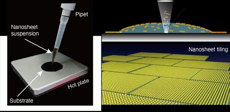
Scientists at Japan’s Nagoya University and the National Institute for Materials Science have found that a simple one-drop approach is cheaper and faster for tiling functional nanosheets together in a single layer. If the process, described in the journal ACS Nano, can be scaled up, it could advance development of next-generation oxide electronics.
“Drop casting is one of the most versatile and cost-effective methods for depositing nanomaterials on a solid surface,” says Nagoya University materials scientist Minoru Osada, the study’s corresponding author. “But it has serious drawbacks, one being the so-called coffee-ring effect: a pattern left by particles once the liquid they are in evaporates. We found, to our great surprise, that controlled convection by a pipette and a hotplate causes uniform deposition rather than the ring-like pattern, suggesting a new possibility for drop casting.”
The process Osada describes is surprisingly simple, especially when compared to currently available tiling techniques, which can be costly, time-consuming, and wasteful. The scientists found that dropping a solution containing 2D nanosheets with a simple pipette onto a substrate heated on a hotplate to a temperature of about 100°C, followed by removal of the solution, causes the nanosheets to come together in about 30 seconds to form a tile-like layer.
Analyses showed that the nanosheets were uniformly distributed over the substrate’s surface, with limited gaps. This is probably a result of surface tension driving how particles disperse, and the shape of the deposited droplet changing as the solution evaporates.
The scientists used the process to deposit particle solutions of titanium dioxide, calcium niobate, ruthenium oxide, and graphene oxide. They also tried different sizes and shapes of a variety of substrates, including silicon, silicon dioxide, quartz glass, and polyethylene terephthalate (PET). They found they could control the surface tension and evaporation rate of the solution by adding a small amount of ethanol.
Furthermore, the team successfully used this process to deposit multiple layers of tiled nanosheets, fabricating functional nanocoatings with various features: conducting, semiconducting, insulating, magnetic and photochromic.
“We expect that our solution-based process using 2D nanosheets will have a great impact on environmentally benign manufacturing and oxide electronics,” says Osada. This could lead to next-generation transparent and flexible electronics, optoelectronics, magnetoelectronics, and power harvesting devices.
###
The study, ” Single Droplet Assembly for Two-Dimensional Nanosheet Tiling,” was published online in the journal ACS Nano on October 29, 2020 at DOI: 10.1021/acsnano.0c05434.
About Nagoya University, Japan
Nagoya University has a history of about 150 years, with its roots in a temporary medical school and hospital established in 1871, and was formally instituted as the last Imperial University of Japan in 1939. Although modest in size compared to the largest universities in Japan, Nagoya University has been pursuing excellence since its founding. Six of the 18 Japanese Nobel Prize-winners since 2000 did all or part of their Nobel Prize-winning work at Nagoya University: four in Physics – Toshihide Maskawa and Makoto Kobayashi in 2008, and Isamu Akasaki and Hiroshi Amano in 2014; and two in Chemistry – Ryoji Noyori in 2001 and Osamu Shimomura in 2008. In mathematics, Shigefumi Mori did his Fields Medal-winning work at the University. A number of other important discoveries have also been made at the University, including the Okazaki DNA Fragments by Reiji and Tsuneko Okazaki in the 1960s; and depletion forces by Sho Asakura and Fumio Oosawa in 1954.
Website: http://en.
Media Contact
Minoru Osada
[email protected]
Original Source
http://en.
Related Journal Article
http://dx.


