


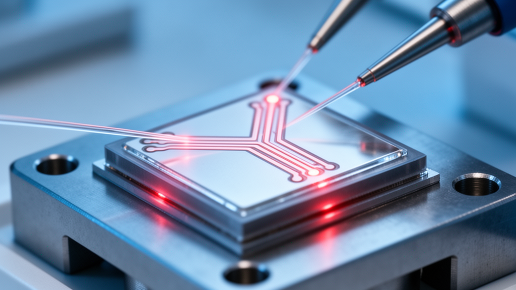
A team of photonic engineers has designed, fabricated and tested a compact 1 × 2 optical power splitter on an indium phosphide platform that achieves an actual splitting loss of approximately 3.3 decibels, excluding coupling losses, alongside a power uniformity better than 0.05 decibels between its two output channels. The device, built on a ridge waveguide structure in the InP/InGaAsP material system, was reported to maintain an insertion loss below 4 decibels across a wide operating band around the 1550 nanometer telecommunications wavelength. The work addresses a fundamental building block for photonic integrated circuits, the basic splitter unit from which larger multi-channel splitting networks are cascaded, and demonstrates performance characteristics that the researchers argue are well matched to the demands of coherent optical communications and dense wavelength division multiplexing systems.
The splitter belongs to a device family known as multimode interference, or MMI, couplers. These components exploit the self-imaging effect: when light enters a waveguide wide enough to support many transverse modes, those modes travel at different phase velocities, and their superposition periodically reconstructs the input optical field at defined distances along the guide. At particular lengths, the field appears as a single replica of the input; at others, it appears as several equal-intensity images. A 1 × 2 MMI splitter places its output waveguides precisely at the two image points, so that the incoming light divides evenly between them. The approach offers a compact footprint, low insertion loss, generous fabrication tolerances and polarization insensitivity, which explains why MMI structures have long served as workhorses for signal distribution and multiplexing in optical networks.
The choice of material platform is central to the design. InP/InGaAsP offers strong optical confinement and favorable electrical properties in the 1550 nanometer window, and unlike passive platforms such as silicon-on-insulator, thin-film lithium niobate or aluminum oxide, it allows lasers and modulators to be monolithically integrated on the same chip. The researchers note that InP-based devices benefit from a higher refractive index contrast than alternatives such as silica-on-silicon or lithium niobate, enabling more compact device dimensions while retaining excellent thermal stability and electro-optic modulation capability. In the demonstrated device, the epitaxial stack comprised an InP substrate, a 200-nanometer InP lower cladding, a 400-nanometer InGaAsP core with a refractive index of roughly 3.4 at 1550 nanometers, and an InP upper cladding, topped by a 1.5-micrometer p-type InP ridge waveguide layer.
A key structural decision was the use of a shallowly etched ridge waveguide rather than a deeply etched one. Deep etching yields strong optical confinement but exposes the waveguide to significant scattering loss from sidewall roughness and demands more complex processing. By etching only through the p-type ridge layer to a depth of about 1.5 micrometers and leaving the core region intact, the team preserved sufficient confinement while reducing sidewall scattering, lowering polarization-dependent loss and relaxing sensitivity to etching-depth fluctuations, all of which improve manufacturing yield. The ridge was patterned using a silicon dioxide hard mask and dry etching, with the researchers reporting excellent sidewall morphology in scanning electron microscope images of the finished devices.
Because the splitter’s performance is acutely sensitive to geometry, the team carried out extensive three-dimensional finite-difference time-domain simulations, using a variational optimization approach, to identify the optimal dimensions. Theory showed that a theoretical optimum exists for the MMI length, at which the two output images are perfectly balanced and loss is minimized; deviations degrade the self-imaging and inflate both imbalance and loss. Simulations indicated that additional loss could be kept below 0.5 decibels within a deviation of plus or minus 5 percent from the optimal length. Sweeping the MMI width from 7.0 to 7.5 micrometers revealed a peak output intensity of 0.471 per channel at 7.3 micrometers, where mode excitation and phase matching are jointly optimized. Below that width, too few modes are excited to produce strong interference; above it, extra high-order modes shift the self-imaging position and leak power into radiation.
The device length showed a similarly forgiving behavior. The simulated optimum was 61 micrometers, and between 54 and 71 micrometers the output intensity varied by only about 3.8 percent, a tolerance the authors describe as extremely favorable for semiconductor processing. The position of the output waveguides also mattered: with a 7.3-micrometer-wide, 61-micrometer-long multimode region, the output intensity peaked when the waveguides sat 2.2 micrometers from the device centerline, and varied by roughly 4 percent over a 0.4-micrometer offset range before falling off sharply as the guides drifted out of the high-intensity region of the self-image. Input and output waveguides were designed to be strictly single-mode, with simulations showing that the first higher-order mode appears only once ridge width exceeds about 3 micrometers, ensuring a pure fundamental-mode field enters the interference region.
Fabrication took place on a 2-inch InP epitaxial wafer, using photolithography and inductively coupled plasma etching to transfer the ridge pattern, first into the silicon dioxide mask and then into the semiconductor itself, followed by a wet-etch mask removal. To characterize the device, the team prepared three chip types: straight waveguides of varying lengths to measure propagation and coupling losses; chips combining straight and 7-millimeter-radius bend waveguides, whose bend loss was negligible; and the complete splitter chips, with outputs spaced 250 micrometers apart for fiber access. Using a 1550 nanometer laser source and an optical power meter, and applying a cut-back method with linear regression across straight waveguides from 500 to 2000 micrometers, they extracted a propagation loss of 2.7 decibels per centimeter and a combined input-output coupling loss of 11.24 decibels, with a fitting coefficient of determination of 0.97 indicating stable sidewall-scattering-dominated loss.
Measured performance of the splitter chips closely tracked the simulations. The loss in each output channel first decreased and then increased as width and length were varied, and a minimum insertion loss of approximately 14.5 decibels was reached at an MMI width of 7.2 micrometers and length of 62 micrometers. Subtracting the fiber coupling losses, the intrinsic device loss came to about 3.3 decibels, close to the theoretical 3-decibel limit imposed by splitting the power in two. Across the tested geometries, the difference between the two output channels remained below 0.1 decibel, and at the optimum the power uniformity was better than 0.05 decibel, confirming accurate placement of the self-imaging point and precise dimensional control during fabrication.
The researchers acknowledge that rival passive platforms, including thin-film lithium niobate, silicon and polymer devices, have demonstrated ultra-compact footprints and, in some cases, lower insertion losses than the 3.3 decibels reported here. What the InP/InGaAsP ridge design offers instead is exceptional splitting uniformity, which becomes critical when many 1 × 2 units are tree-cascaded into larger networks, where even small imbalances accumulate, and when the splitter serves inside Mach-Zehnder modulators or interferometric switches, where sub-decibel imbalance can sharply degrade extinction ratios. Combined with the ability to integrate the splitter monolithically with lasers and modulators in the same 1550 nanometer band, the team positions the device as a candidate fundamental passive component for integrated multi-wavelength light sources and broadband WDM systems, with future work targeting reduced end-face coupling loss, broader operating bandwidth and systematic testing of cascaded splitter networks.
Subject of Research: Design and fabrication of a low-loss 1 × 2 multimode interference power splitter on an InP/InGaAsP ridge waveguide platform
Article Title: Characteristics of a 1 × 2 multimode interference splitter based on low-loss InP/InGaAsP ridge waveguide for photonic integration
Article References: Wang, J., Zhang, Y., Wei, Y., Chu, K., Zheng, Z., Gao, F., Zheng, W., Hong, Q., Zhao, S., Chang, X., & Huang, Y. (2026). Characteristics of a 1 × 2 multimode interference splitter based on low-loss InP/InGaAsP ridge waveguide for photonic integration. Results in Optics, Article 101185. https://doi.org/10.1016/j.rio.2026.101185
Image Credits: AI Generated
DOI: 10.1016/j.rio.2026.101185
Keywords: photonic integrated circuits, multimode interference splitter, InP/InGaAsP, ridge waveguide, insertion loss, power uniformity, self-imaging effect, 1550 nm, wavelength division multiplexing, FDTD simulation, reactive ion etching, Mach-Zehnder modulator
News Source: Denise Maddox. (October 23, 2026). Low-Loss InP Splitter Delivers Near-Perfect Power Balance for Photonic Chips. Scienmag.