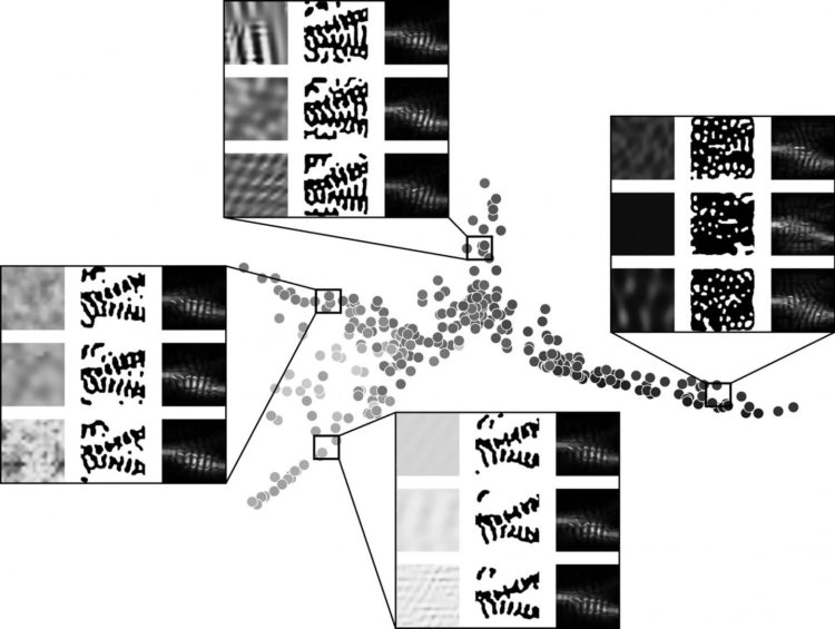
Better design optimization of optical and photonic components may speed their commercial viability and open new possibilities for a wide range of integrated photonics

Credit: Logan Su
WASHINGTON, March 10, 2020 — Stanford University researchers created an inverse design codebase called SPINS that can help researchers explore different design methodologies to find fabricable optical and nanophotonic structures.
In the journal Applied Physics Reviews, from AIP Publishing, Logan Su and colleagues review inverse design’s potential for optical and nanophotonic structures, as well as present and explain how to use their own inverse design codebase.
“The idea of inverse design is to use more sophisticated optimization algorithms and automate the search for a structure,” Su explained. “The ultimate goal is to have a designer input their desired performance metrics and simply wait for the algorithm to generate the best possible device.”
Integrated photonics has many potential applications, ranging from optical interconnects to sensing to quantum computing.
Inspired by popular machine learning libraries such as TensorFlow and PyTorch, SPINS is a photonic design framework that emphasizes flexibility and reproducible results. SPINS has been used internally by the group to design an assortment of devices, and the group is making it available for other researchers to use.
“The mathematics behind our optimization techniques come from the mathematical optimization community,” Su said. “But we also borrow ideas from the optimization community in mechanical and fluid mechanics, where they use similar optimization methods to design mechanical structures and airfoils before their adoption in photonics.”
Inverse design “automates the design process for optical and photonic elements,” he said. “Traditionally, photonic devices are hand designed, in the sense that a designer first comes up with the basic geometric shape of the structures, such as a circle, and then performs a few parameter sweeps of the radius of the circle to improve device performance.”
This process is labor intensive and tends to ignore a large class of devices with more complicated shapes that have the potential for much better performance.
“Replacing electrical interconnects with photonic interconnects within data centers, for example, could enable an increase in memory bandwidth while substantially decreasing energy costs,” Su said.
Photonic neural networks also promise faster operation speeds with lower energy requirements compared to electronic hardware, and metasurface optics promise novel optical functionalities that are cheaper and orders of magnitude smaller than their traditional bulky optical elements.
“Part of the barrier to the adoption of these technologies is the performance of the photonic components that comprise that system,” Su said. “By developing a better optimization method for designing these photonic components, we hope to not only improve the performance of these technologies to the point of commercial viability but also open up new possibilities for integrated photonics.”
###
The article, “Nanophotonic inverse design with SPINS: Software architecture and practical considerations,” is authored by Logan Su, Dries Vercruysse, Jinhie Skarda, Neil V. Sapra, Jan A. Petykiewicz and Jelena Vučkovi?. It will appear in Applied Physics Reviews, March 10, 2020 (DOI: 10.1063/1.5131263). After that date, it can be accessed at https:/
ABOUT THE JOURNAL
Applied Physics Reviews features articles on significant and current topics in experimental or theoretical research in applied physics, or in applications of physics to other branches of science and engineering. The journal publishes both original research on pioneering studies of broad interest to the applied physics community, and reviews on established or emerging areas of applied physics. See https:/
Media Contact
Larry Frum
[email protected]
301-209-3090
Related Journal Article
http://dx.


