New encapsulation technique protects electronic properties of sensitive materials
Credit: HZDR / Sahneweiß
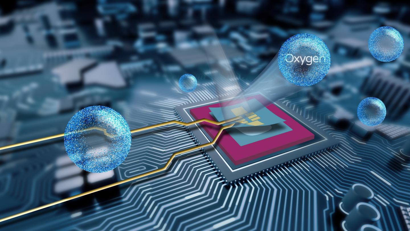
Tomorrow’s electronics are getting ever smaller. Researchers are thus searching for tiny components that function reliably in increasingly narrow configurations. Promising elements include the chemical compounds indium selenide (InSe) and gallium selenide (GaSe). In the form of ultra-thin layers, they form two-dimensional (2D) semi-conductors. But, so far, they have hardly been used because they degrade when they get in contact with air during manufacturing. Now, a new technique allows the sensitive material to be integrated in electronic components without losing its desired properties. The method, which has been described in the journal ACS Applied Materials and Interfaces (DOI: 10.1021/acsami.9b13442), was developed by Himani Arora, a doctoral candidate of physics at the Helmholtz-Zentrum Dresden-Rossendorf (HZDR).
“We managed to make encapsulated transistors based on indium selenide and gallium selenide,” reports Dr. Artur Erbe, head of the “Transport in Nanostructures” group at HZDR’s Institute of Ion Beam Physics and Materials Research. “The encapsulation technique protects the sensitive layers from external impacts and preserves its performance.” For encapsulation, the scientists use hexagonal boron nitride (hBN). It is ideal for the purpose because it can be formed into a thin layer and is also inert, so it does not respond to its environment.
Indium and gallium selenide are seen as promising candidates for various applications in areas such as high-frequency electronics, optoelectronics and sensor technology. These materials can be made into flake-like films only 5 to 10 atomic layers thick which can be used to produce electronic components of extremely small dimensions.
During encapsulation, the 2D flakes are arranged between two layers of hexagonal boron nitride and thus completely enclosed. The upper hBN layer is responsible for outward insulation, the lower one for maintaining distance to the substrate. The technique was originally developed by the group of James Hone at Columbia University in New York where Himani Arora learned it during a research visit. The doctoral student subsequently continued to work on the topic at HZDR’s International Helmholtz Research School (IHRS) NanoNet.
Applying contacts without lithography
One of the particularly big challenges posed by the encapsulation technique was to apply external contacts to the semi-conductors. The usual method of evaporation deposition using a photomask is unsuitable because during this process the sensitive materials come into contact both with chemicals and with air and thus degrade. So, the HZDR researchers employed a lithography-free contacting technique involving metal electrodes made of palladium and gold embedded in hBN foil. This means the encapsulation and the electric contact with the 2D layer underneath can be achieved concurrently.
“In order to produce the contacts, the desired electrode pattern is etched onto the hBN layer so that the holes created can be filled with palladium and gold by means of electron beam evaporation,” Himani Arora explains. “Then you laminate the hBN foil with the electrodes onto the 2D flake.” When there are several contacts on an hBN wafer, contact with several circuits can be made and measured. For later application, the components will be stacked in layers.
As the experiments have shown, complete encapsulation with hexagonal boron nitride protects the 2D layers from decomposition and degradation and ensures long-term quality and stability. The encapsulation technique developed at HZDR is robust and easy to apply to other complex 2D materials. This opens up new paths for fundamental studies as well as for integrating these materials into technological applications. The new two-dimensional semi-conductors are cheap to produce and can be used for various applications such as detectors that measure light wavelengths. Another example of use would be as couplers between light and electronic current by generating light or switching transistors using light.
###
This study was made available online in October 2019 ahead of final publication in issue in November 2019.
Publication:
H. Arora, Y. Jung, T. Venanzi, K. Watanabe, T. Taniguchi, R. Hübner, H. Schneider, M. Helm, J. C. Hone, A. Erbe: Effective hexagonal boron nitride passivation of few-layered InSe and GaSe to enhance their electronic and optical properties, in ACS Applied Materials & Interfaces, 2019 (DOI: 10.1021/acsami.9b13442)
Further information:
PD Dr. Artur Erbe | Himani Arora
Institute of Ion Beam Physics and Materials Research
Phone: +49 351 260-2366
Mail: [email protected] | [email protected]
Media contact:
Simon Schmitt | Science editor
Phone: +49 351 260-3400 | Email: [email protected]
Helmholtz-Zentrum Dresden-Rossendorf | Bautzner Landstr. 400 | 01328 Dresden / Germany | http://www.
The Helmholtz-Zentrum Dresden-Rossendorf (HZDR) performs – as an independent German research center – research in the fields of energy, health, and matter. We focus on answering the following questions:
- How can energy and resources be utilized in an efficient, safe, and sustainable way?
- How can malignant tumors be more precisely visualized, characterized, and more effectively treated?
- How do matter and materials behave under the influence of strong fields and in smallest dimensions?
To help answer these research questions, HZDR operates large-scale facilities, which are also used by visiting researchers: the Ion Beam Center, the High-Magnetic Field Laboratory Dresden, and the ELBE Center for High-Power Radiation Sources.
HZDR is a member of the Helmholtz Association and has five sites (Dresden, Freiberg, Grenoble, Leipzig, Schenefeld near Hamburg) with almost 1,200 members of staff, of whom about 500 are scientists, including 170 Ph.D. candidates.
Media Contact
Simon Schmitt
[email protected]
49-351-260-3400
Original Source
http://www.
Related Journal Article
http://dx.


