This enables observation inside hard materials with an atomic-scale
Credit: NIFS
A research team of fusion scientists has succeeded in developing “the nano-scale sculpture technique” to fabricate an ultra-thin film by sharpening a tungsten sample with a focused ion beam. This enables the nano-scale observation of a cross-section very near the top surface of the tungsten sample using the transmission electron microscope. The sculpture technique developed by this research can be applied not only to tungsten but also to other hard materials.
Hardened materials such as metals, carbons and ceramics are used in automobiles, aircraft and buildings. In a fusion reactor study, “tungsten,” which is one of the hardest metal materials, is the most likely candidate for the armour material of the device that receives the plasma heat/particle load. This device is called divertor. In any hardened materials, nanometer scale damages or defects can be formed very near the top surface of the materials. For predicting a material lifetime, it is necessary to know the types of the damages and their depth profiles in the material. To do this, we must observe a cross-section of the region very near the top surface of the material with nano-scale level.
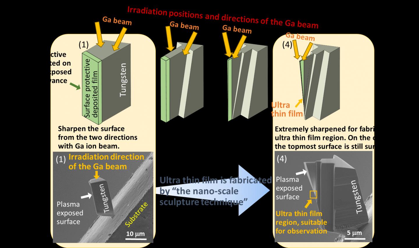
For the observation of the internal structure of materials with nano-scale level, transmission electron microscope (TEM), in which accelerated electrons are transmitted through the target materials, is commonly used as a powerful tool. In order to observe a cross-section very near the top surface of the tungsten with TEM, we firstly extract a small piece of the tungsten sample from its surface and then fabricate an ultra-thin film by cutting the extracted sample. The thickness of the film must be below ~100 nm (nanometer) to obtain high resolution due to the high-transmission of the electron beam (IMAGE 1). However, it has been extremely difficult to fabricate such an ultra-thin film for the hard materials such as a tungsten. Therefore, it has been almost impossible to obtain the ~100 nm thickness level by using conventional thin-film fabrication technique.
The research team of Dr. Masayuki Tokitani and Daisuke Nagata et al. of the National Institutes of Natural Sciences (NINS) National Institute for Fusion Science (NIFS) have developed a superior nano-scale fabrication technique for tungsten, by using a focused ion beam – electron beam (FIB-SEM) device. They call this technique “the nano-scale sculpture technique.” The FIB-SEM device enables us to cut materials by irradiating them with a focused Ga ion beam with the size of ~30 nm in diameter. The research team previously tried to fabricate an ultra-thin film by sharpening the small piece of the tungsten with FIB-SEM. However, they had the problem that the topmost surface was unfortunately lost because the beam intensity had to be relatively strong for the hard tungsten. To solve this problem, they have now produced a special Ga beam operation to maintain the topmost surface by adjusting the beam irradiation positions and directions. They also gradually sharpen the region near the surface, creating a shape that becomes thinner toward the bottom. Consequently, they obtain an ultra-thin film with the thickness of ~100 nm or less and with the top surface remaining (IMAGE 2).
In the image obtained by the TEM observation of the fabricated ultra-thin film (IMAGE 3), we can clearly identify the atomic level damages formed near the top surface of the tungsten sample. Thus, “the nano-scale sculpture technique” developed by this research team makes it possible to observe a cross-section near the top surface of the tungsten sample with an atomic-scale. This sculpture technique can be applied not only to tungsten but also to other hard materials such as hardened alloys and ceramics. Currently, we are considering this sculpture technique for application to the automobile industry.
###
Key Words
(1) Divertor
In the nuclear fusion reactor, the divertor has the function of maintaining the purity of a nuclear fusion plasma by neutralizing the charged particles of impurities including fuel gas particles flowing along the magnetic field lines and by exhausting them. Conversely, because the kinetic energy of the charged particles becomes heat on the divertor surface, this place continuously receives the highest heat load.
(2) Focused ion beam – electron beam fabrication device (FIB-SEM)
The nano-scale fabrication device for creating an ultra-thin film sample for TEM observation by using the focused Ga ion beam.
Media Contact
Dr. Masayuki Tokitani
[email protected]

