Osaka Prefecture University develops a method to design and control the path of electron flow in a polycrystalline material
Credit: ©M. TAKAHASHI & K. OKADA, OSAKA PREFECTURE UNIVERSITY
Metal-organic frameworks (MOF) are crystalline porous organic-inorganic hybrid materials that, by filling its pores with guest molecules, can create functionalities through interactions between the organic-inorganic based frameworks of MOF (host) and its guest molecules. This host-guest chemistry has the potential to bring “designable” electrical properties, allowing for a material to be organized in ways never before possible – paving the way for the next-generation of thin-film smart devices.
“However, most MOFs exhibit poor electrical conductivity”, states Professor Masahide Takahashi, “due to the insulating nature of the organic linkers and the gaps between the varied shapes that make up the crystalline material.” His research group from the Osaka Prefecture University, Graduate School of Engineering has developed a method to design and control the path of electron flow in a polycrystalline material and have realized a thin film material that shows high conductivity in a controllable direction. Their work was reported on June 4th, 2021, in the Journal of Materials Chemistry A.
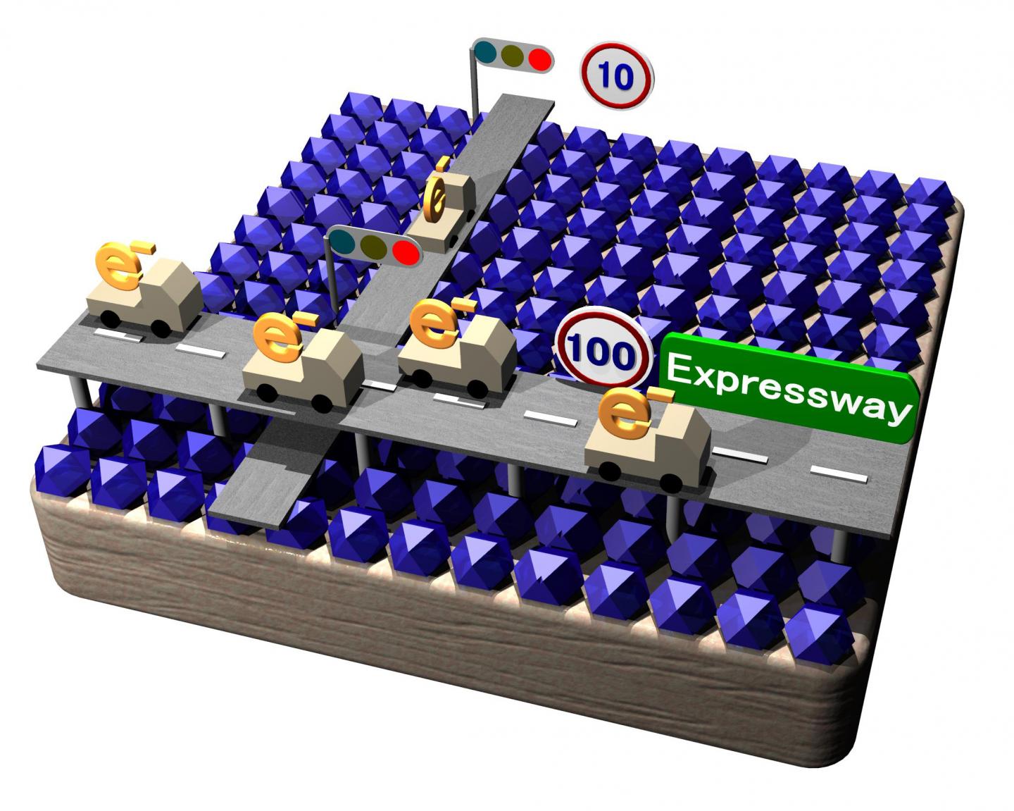
First, consider the electron flow created by the interaction between the host MOF and its guest molecules. Imagine a host material made up of a same-shaped crystal – like a pristine single-crystal conductor. As the entire mass is one shape, there would be no gaps between its guest molecules and thus great conductivity. The downside is that processing this material to manufacture other devices would require high temperatures and pressure and precise control of the atmosphere to maintain its uniform shape. So far this has proved unpractical. A polycrystalline material is made up of small crystals of varying size and shape. This frees it of same hurdle of maintaining a uniform shape during processing, making it a candidate material for the manufacture of a wide range of next-gen thin film devices. However, “to exhibit similar conductivity functions as single crystals, we would need a method of aligning the crystal grains without gaps” states Associate Professor Kenji Okada.
These crystal grains in MOFs are like molecular-sized pores that can accommodate specific molecules at a specific orientation and spacing. Instead of figuring out how to align the shape of each pore to each molecule to facilitate conductivity, the team focused on the regularities of the surface hydroxyl groups of the metal hydroxides. Using a combination of lattice matching and interface bonding, the team determined two types of orientation relationships, or conductive paths, and realized an orientation where the in-plane path was 10 times more conductive than the other.
“By combining the epitaxial growth approach with UV lithography technology,” states Professor Takahashi, “we were able to create oriented semiconducting polycrystalline MOF films regardless to the shape of the individual crystals.”
###
Paper title: Oriented growth of semiconducting TCNQ@Cu3(BTC)2 MOF on Cu(OH)2: crystallographic orientation and pattern formation toward semiconducting thin-film devices
About Osaka Prefecture University, Japan
Osaka Prefecture University (OPU) is one of the largest public universities in Japan.
OPU comprises three campuses, with a main campus in Sakai, Osaka. With four colleges for undergraduate students and seven graduate schools, the university offers stellar education in a myriad of fields like engineering, life and environmental sciences, science, economics, humanities and social sciences, and nursing. Not just this, the university also houses various international students, who can enrich their lives with opportunities for internships and exchange programs.
In April 2022, OPU will unite with Osaka City University (OCU) to form Japan’s largest public university, Osaka Metropolitan University (tentative name).
For more details, please visit:
Osaka Prefecture University (OPU): https:/
Osaka Metropolitan University (tentative name): https:/
Media Contact
Yoshiko Tani
[email protected]
Original Source
https:/
Related Journal Article
http://dx.


