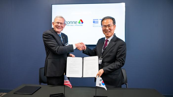

Korean researchers have embarked on an ambitious journey to collaborate closely with the U.S. Department of Energy’s Argonne National Laboratory (ANL) focused on semiconductor technology research. This collaboration, formalized through a Memorandum of Understanding (MOU) signed on January 6, marks a significant step forward in the development of advanced semiconductor technologies, particularly those applicable to high-energy particle detection and analysis.
The Electronics and Telecommunications Research Institute (ETRI), an influential player in Korea’s research landscape, announced this partnership, emphasizing the potential for shared knowledge and technological innovations. ETRI is renowned for its pioneering work in semiconductor technologies, particularly in the development and production of silicon detectors for high-energy physics applications. Since the early 2000s, ETRI has been the sole government-funded institute in Korea capable of silicon batch processing, making it a vital contributor to the nation’s technological advancements.
In recent years, ETRI and ANL have quietly collaborated, focusing their efforts on developing a monolithic active pixel sensor (MAPS). This state-of-the-art technology utilizes complementary metal-oxide semiconductor (CMOS) integrated circuits (ICs) to enhance the performance and accuracy of high-energy particle detectors. The new MOU is set to build upon this foundation, paving the way for further technological advancements that can significantly enhance our understanding of high-energy particles, particularly those originating from space environments.
As the partnership solidifies, ETRI and ANL are poised to make substantial progress in the realm of semiconductor technology. The shared goal is to develop highly sensitive detectors capable of withstanding harsh environmental conditions found in space. These detectors will not only advance scientific research but also have practical applications in various fields, including aerospace and defense. The collaboration promises to harness the expertise from both organizations, combining ANL’s extensive research capabilities with ETRI’s cutting-edge technological innovations.
The remarks made by Bang Seung Chan, the president of ETRI, reflect the optimism surrounding this collaboration. He articulated the significance of the MOU, emphasizing that it uniquely combines the expert capabilities of ANL with ETRI’s technologies. This collaboration is anticipated to create new opportunities in semiconductor research and development, facilitating advancements that could redefine our understanding of particle physics and its applications.
Paul Kearns, the director of ANL, echoed these sentiments, expressing hope that the expanding collaboration would cover various technological fields, including the Electron-Ion Collider (EIC) project. The EIC is an ambitious experimental device designed to deepen our understanding of matter’s fundamental structure. By accelerating electrons to collide with ions, researchers aim to explore the complexities of particle interactions, contributing to our fundamental knowledge of the universe.
Through this MOU, ETRI aims to spearhead the domestic manufacturing of semiconductor detectors, striving to enhance Korea’s competitiveness in this critical field. The initiative intends to develop technologies robust enough to endure the extreme conditions of space, which often involve wide temperature fluctuations and exposure to intense radiation. The strategic goal is to foster industrialization in the semiconductor sector, particularly in applications relevant to aerospace and defense.
On the signing day, ETRI took proactive steps to engage with local researchers by organizing a meeting with approximately ten Korean scientists at ANL. The gathering served as a platform to exchange perspectives on local research activities and international R&D cooperation, assessing mutual cooperation plans essential for driving the joint initiative forward.
Semiconductors play an integral role in advancing technology across various domains, making the development of innovative detectors a pressing need. A silicon detector, for instance, serves as a critical tool in detecting charge carriers generated by radiation and photons, making it fundamental for applications in both scientific research and practical deployments.
Understanding the silicon batch process further showcases the complex yet fascinating world of semiconductor manufacturing. This intricate procedure encompasses hundreds of steps, culminating in the fabrication of silicon-based semiconductor chips that serve as the backbone of many modern-day technologies. The precision and control afforded by this process are essential for developing high-performance detectors.
Moreover, the MAPS technology offers a revolutionary approach to monitoring and detecting high-energy particles with enhanced accuracy. By integrating a detector with a CMOS IC, MAPS technology provides a comprehensive solution that advances both the detection and processing of particle-generated signals. This synergy paves the way for innovative applications in various scientific fields.
The potential of this collaboration, therefore, cannot be overstated. The convergence of ETRI’s expertise in silicon-based technologies and ANL’s extensive research capabilities will likely yield unprecedented breakthroughs in semiconductor technology. The implications could extend beyond theoretical applications, influencing practical implementations in fields such as climate monitoring, space exploration, and beyond.
As excitement builds around this ambitious international collaboration, the scientific community and industry stakeholders will be closely watching the outcomes. The successful development of semiconductor technologies that can detect and analyze high-energy particles in space would not only elevate Korea’s status in the global technology landscape but also enhance the capabilities of research entities worldwide.
In conclusion, the MOU symbolizes a promising union between ETRI and ANL, merging their strengths in semiconductor research. As both parties move forward, the advent of new technologies that arise from this partnership will aim to resolve some of the most compelling questions in modern physics, while simultaneously contributing to advancements that can withstand the rigors of extreme environments, ensuring their relevance for years to come.
Subject of Research: Semiconductor Technology Collaboration
Article Title: Korea and Argonne National Laboratory Forge New Semiconductor Partnership
News Publication Date: January 6, 2023
Web References: www.etri.re.kr
References: None
Image Credits: Electronics and Telecommunications Research Institute (ETRI)
Keywords
Semiconductor technology, high-energy particles, ETRI, Argonne National Laboratory, MOU, MAPS, CMOS, research collaboration, aerospace, defense, silicon detectors, Electron-Ion Collider, particle physics.
Tags: advancements in particle analysis technologyCMOS integrated circuits in particle detectionETRI Argonne National Laboratory partnershipETRI contributions to semiconductor industryhigh-energy particle detection advancementshigh-energy physics technology improvementsKorea U.S. research collaborationMemorandum of Understanding ETRI ANLmonolithic active pixel sensor developmentsemiconductor technology research collaborationsilicon detectors for high-energy physicstechnological innovations in semiconductors

