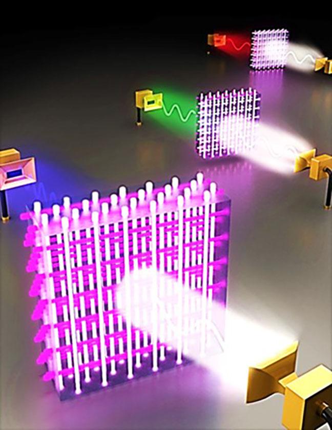
Researchers have painstakingly combined plasma, metal and dielectric materials into multifunctional, artificial crystals, which could pave the way to higher bandwidth wireless communications

Credit: Image courtesy of the University of Illinois
WASHINGTON, D.C., December 10, 2019 — Scientists at the University of Illinois have created sugar cube-sized blocks of an electromagnetic material with potential to transform communication networks.
Several countries are building futuristic communication systems using higher frequency electromagnetic waves to transfer more data at faster rates, but they have lacked network components to handle these higher bandwidths. Researcher J. Gary Eden proved his new device can rapidly switch functionality to perform the varied tasks needed to support a network with carrier frequencies of over 100 gigahertz. The miniscule-scale architecture concealed within the sugar cube blocks is described in Applied Physics Reviews, from AIP Publishing.
“This technology is particularly interesting, because it generates multiple channels operating simultaneously at different frequencies. Basically, this allows multiple conversations to occur over the same network, which is the heart of high-speed wireless communications,” explained Eden.
Plasma is critical for swiftly switching between functions and frequencies, but previous plasma-based electromagnetic crystals were much too large to operate at high frequencies. The key lies in creating a structure with spacing between the plasma and metal columns as small as the wavelength of radiation being manipulated.
The wavelength of electromagnetic waves shortens as the frequency and bandwidth increase. To realize crystals of high bandwidth operating at frequencies above 100 GHz, a small-scale design is required.
Eden’s team developed a 3D-printed scaffold, which served as a negative of the desired network. A polymer was poured in and, once set, microcapillaries 0.3 millimeters in diameter were filled with plasma, metal or a dielectric gas. Using this replica-molding technique, it took nearly five years to perfect the dimensions and spacings of the microcapillaries in the woodpilelike lattice.
“Assembling the material was extremely demanding,” said Eden, but eventually, he and his team were able to use their material to observe resonance spanning the 100 GHz to 300 GHz frequency region, which Eden noted as “an enormous spectral range over which to operate.”
The group showed that rapid changes in the electromagnetic characteristics of these crystals — such as switching between reflecting or transmitting signals — could be achieved by simply turning on or off a few plasma columns. Such a capability shows the utility of such a dynamic and energy-efficient device for communications.
Eden is keen to further optimize the fabrication and switching efficiencies of this new device but is also excited to delve into other applications. For instance, the crystal could be tuned to respond to the resonances of specific molecules, e.g., atmospheric pollutants, and be used as a highly sensitive detector.
###
The article, “Dynamic plasma/metal/dielectric photonic crystals in the mm-wave region: Electromagnetically-active artificial material for wireless communications and sensors,” is authored by Peter P. Sun, Runyu Zhang, Wenyuan Chen, Paul V. Braun and J. Gary Eden. The article will appear in the journal Applied Physics Reviews on Dec. 10, 2019 (DOI: 10.1063/1.5120037). After that date, it can be accessed at https:/
ABOUT THE JOURNAL
Applied Physics Reviews features articles on significant and current topics in experimental or theoretical research in applied physics, or in applications of physics to other branches of science and engineering. The journal publishes both original research on pioneering studies of broad interest to the applied physics community, and reviews on established or emerging areas of applied physics. See https:/
Media Contact
Larry Frum
[email protected]
301-209-3090
Related Journal Article
http://dx.


