Credit: Magnus Johansson/Linköping University
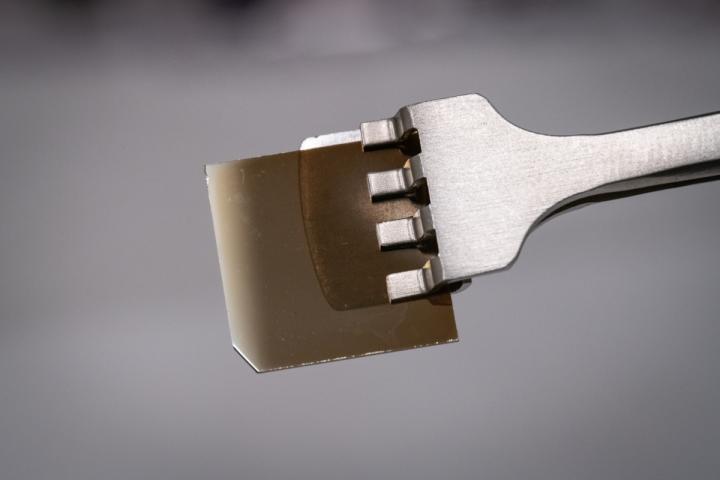
Indium nitride is a promising material for use in electronics, but difficult to manufacture. Scientists at Linköping University, Sweden, have developed a new molecule that can be used to create high-quality indium nitride, making it possible to use it in, for example, high-frequency electronics. The results have been published in Chemistry of Materials.
The bandwidth we currently use for wireless data transfer will soon be full. If we are to continue transmitting ever-increasing amounts of data, the available bandwidth must be increased by bringing further frequencies into use. Indium nitride may be part of the solution.
“Since electrons move through indium nitride extremely easily, it is possible to send electrons backwards and forwards through the material at very high speeds, and create signals with extremely high frequencies. This means that indium nitride can be used in high-frequency electronics, where it can provide, for example, new frequencies for wireless data transfer”, says Henrik Pedersen, professor of inorganic chemistry at the Department of Physics, Chemistry and Biology at Linköping University. He has led the study, which was recently published in Chemistry of Materials.
Indium nitride consists of nitrogen and a metal, indium. It is a semiconductor and can therefore be used in transistors, on which all electronic devices are based. The problem is that it is difficult to produce thin films of indium nitride. Thin films of similar semiconductor materials are often produced using a well-established method known as chemical vapour deposition, or CVD, in which temperatures between 800 and 1,000 degrees Celsius are used. However, indium nitride breaks down into its constituents, indium and nitrogen, when it is heated above 600 degrees Celsius.
The scientists who conducted the present study have used a variant of CVD known as atomic layer deposition, or ALD, in which lower temperatures are used. They have developed a new molecule, known as an indium triazenide. No one had worked with such indium triazenides previously, and the LiU researchers soon discovered that the triazenide molecule is an excellent starting material for the manufacture of thin films. Most materials used in electronics must be produced by allowing a thin film to grow on a surface that controls the crystal structure of the electronic material. The process is known as epitaxial growth. The researchers discovered that it is possible to achieve epitaxial growth of indium nitride if silicon carbide is used as substrate, something that was not previously known. Furthermore, the indium nitride produced in this way is extremely pure, and among the highest quality indium nitride in the world.
“The molecule that we have produced, an indium triazenide, makes it possible to use indium nitride in electronic devices. We have shown that it is possible to produce indium nitride in a manner that ensures that it is sufficiently pure to be described as a true electronic material”, says Henrik Pedersen.
The researchers discovered another surprising fact. It is generally accepted among those who use ALD that the molecules should not be allowed to react or be broken down in any way in the gas phase. But when the researchers changed the temperature of the coating process, they discovered that there is not just one, but two, temperatures at which the process was stable.
“The indium triazenide breaks down into smaller fragments in the gas phase, and this improves the ALD process. This is a paradigm shift within ALD – using molecules that are not fully stable in the gas phase. We show that we can obtain a better final result if we allow the new molecule to break down to a certain extent in the gas phase”, says Henrik Pedersen.
The researchers are now examining similar triazenide molecules with other metals than indium, and have obtained promising results when using these to produce molecules for ALD.
###
The study has been carried out together with researchers from the Swedish University of Agricultural Sciences in Uppsala and Carleton University in Ottawa, Canada. It has received financial support from the Swedish Foundation for Strategic Research (SSF) and the Knut and Alice Wallenberg Foundation. Principal author of the published article is Nathan O´Brien, research fellow in the Department of Physics, Chemistry and Biology at Linköping University.
The article: “In Situ Activation of an Indium(III) Triazenide Precursor for Epitaxial Growth of Indium Nitride by Atomic Layer Deposition”, Nathan J. O’Brien, Polla Rouf, Rouzbeh Samii, Karl Ronnby, Sydney C. Buttera, Chih-Wei Hsu, Ivan G. Ivanov, Vadim Kessler, Lars Ojama?e and Henrik Pedersen, Chemistry of Materials, published as an open access article on 24 April, doi: 10.1021/acs.chemmater.9b05171
Link: https:/
Media Contact
Henrik Pedersen
[email protected]
Original Source
https:/
Related Journal Article
http://dx.


