Credit: by Elena Goi, Xi Chen, Qiming Zhang, Benjamin P. Cumming, Steffen Schoenhardt?Haitao Luan and Min Gu
Today, machine learning based methods are of our everyday life, with millions of users every day unlocking their phones through facial recognition or passing through AI-enabled automated security checks at airports and train stations. Traditionally, the processing of information native to the optical domain is being executed in the electronic domain, requiring energy-hungry specialized electronic hardware and conversion between the two realms. Optical machine learning is emerging as an important field, where the processing of optical information is done directly within the optical domain, power-efficient and at the speed of light.
Machine learning tasks, such as pattern recognition or image classification, rely heavily on the multiplication of large matrices, a resource-hungry computational task. Through machine-learning based design of optical elements with sub-wavelength feature sizes it is possible to perform these matrix operations directly in the optical domain, power-efficient through passive optical components. However, these passive optical elements are currently restricted in neuron size and density, while relying on bulky free-space optical systems, making them unsuitable for optical machine learning tasks in the visible wavelength regime and integration into compact designs.
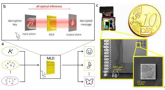
In a new paper published in Light Science & Application, a team of scientists, led by Professor Min Gu from the Centre for Artificial Intelligence Nanophotonics (CAIN), School of Optical, Electrical and Computer Engineering, University of Shanghai for Science and Technology, Shanghai 200093, China, in collaboration with RMIT University in Melbourne (Australia) has developed a new concept for compact optical machine-learning decryptors (MLDs) that process information at the speed of light trough all-optical inference, without consuming any power and can be directly integrated on a CMOS chips. This energy-efficient commixture of optics and electronics paves a path towards machine learning based analysis of optical information for a new generation of edge devices enhanced by artificial intelligence.
In their work, the scientists use computer-based machine learning methods to train thin holographic perceptrons with nanometer feature size, that are capable of recognizing images and perform critical decryption of messages. Using Galvo-Dithered Two Photon Lithography (GD-TPN), a state-of-the-art laser 3D-nanoprinting technology, the researchers fabricate decryptors for operation in the near infrared region with a neuron density of over 500 million neurons per square centimetre with a height resolution down to 10 nm. The nanoscale feature size of these nanoprinted perceptrons not only leads to a higher neuron density and opens the diffractive neural networks up to process information in the visible and near infrared wavelength regime, it also enables highly compact devices through wide diffraction angles and short operative distances. Hence, the upper limit for the computational power for the nanoprinted decryptors lies at 400 ExaFLOPS (1018 FLOPS, floating operations per second), an increase in the operations per second compared with diffractive devices operating in the THz region and integrated photonic hardware of three and five orders of magnitude, respectively.
By printing the MLDs directly on a CMOS chip, the researchers achieve compact and highly integrated devices, which not only outperform current optical decryption methods, but show the potential for application of full optical inference devices in a wide range of fields from computer vision to medical diagnostics. Through the targeted wavelength region, the compactness, the possibility to perform a multitude of tasks, combined with the intrinsic compatibility with electronic-chip manufacturing, including but not limited to CMOS chips, the machine learning decryptors pave the way for a completely new generation of fast and power-efficient functional optical elements for a new generation of edge devices with a wide range of applications.
###
Media Contact
Min Gu
[email protected]
Related Journal Article
http://dx.