


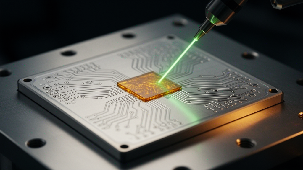
Researchers have demonstrated a way to repair the phase errors that plague large silicon photonic switch matrices after fabrication, using nothing more than focused laser pulses on a thin film of the phase-change material Sb2Se3. The team, reporting in Results in Optics, applied the technique to a complete 4 × 4 Benes switching matrix and showed that it could correct routing errors and suppress crosstalk without any static power consumption, because the material holds its state permanently once switched. The work addresses a well-known bottleneck in silicon photonics: as interferometer-based switching fabrics grow larger, tiny manufacturing deviations accumulate across stages until light is routed to the wrong output ports.
Silicon photonics has become the leading platform for photonic integrated circuits, largely because it is compatible with complementary metal–oxide–semiconductor technology and scales well, making it attractive for the high-bandwidth optical interconnects demanded by data-center infrastructure driven by artificial intelligence workloads. Mach–Zehnder interferometers are key building blocks for optical switching matrices and large-scale switching fabrics, and their broadband response makes them suitable for highly scalable architectures. Their operation, however, depends critically on accurate phase control in each interferometric element. Fabrication-induced variations in waveguide geometry or layer thickness introduce random deviations in the effective index, producing phase errors. In cascaded switching fabrics such as Benes networks, small phase mismatches in individual Mach–Zehnder interferometers accumulate across multiple stages, leading to incorrect routing states and significant crosstalk. Large-scale silicon photonic switching networks therefore require robust post-fabrication phase correction strategies.
Several trimming approaches have been explored to compensate for such phase errors, including ion implantation, polymer claddings, and various thermal treatment methods. While effective, these approaches either require additional fabrication or post-processing steps that increase cost and complexity, or they lack reversibility. Phase-change materials have emerged as a compelling alternative for non-volatile tuning of amplitude and phase in ultra-compact footprints. Some, such as Ge2Sb2Te5, have been widely used in photonic integrated circuits for optical memories and neuromorphic computing, but their non-negligible optical absorption in the telecom bands motivated the search for low-loss chalcogenides such as Sb2Se3. That material offers a wide range of tunability and long-term stability, making it an ideal candidate for phase trimming. Electro-optical phase tuning through integrated heaters is a commonly reported approach, but reversible phase tuning of Sb2Se3 through laser-induced optical excitation has also been demonstrated previously, and it simplifies fabrication by eliminating the need for integrated heaters.
Previous work with phase-change materials focused on the phase tuning of isolated structures, localized laser writing on the material, or the tuning of programmable gate arrays. The new study goes further by demonstrating post-fabrication trimming of a complete Benes switch matrix using an iterative feedback-based approach, experimentally validating error compensation in a scalable switching architecture. The team also demonstrated reversible phase tuning with a resolution of 0.0625π in a symmetric 2 × 2 Mach–Zehnder interferometer built around a 16-micrometre-long hybrid Sb2Se3/silicon waveguide section. In the demonstration, the trimming method compensated for initial phase errors in the 4 × 4 matrix and achieved effective crosstalk suppression without static power consumption.
The fundamental switch element is a symmetric 2 × 2 Mach–Zehnder interferometer in which the phase-tuning section is a hybrid waveguide: a 450 by 220 nanometre silicon waveguide covered by a 40-nanometre-thick layer of Sb2Se3. The phase-change layer has a total width of 5 micrometres to ensure the waveguide top is fully covered against potential mask misalignments during lithography. The refractive index difference between the amorphous and crystalline states of Sb2Se3 modulates the effective index of the guided mode, enabling non-volatile reconfigurability of the switch. Each interferometer incorporates two phase-change patches, one dedicated to path reconfiguration of the matrix and the other to optical trimming. The hybrid waveguide length was chosen to produce a π phase shift between the two states of the material. Multimode interferometers serve as splitters and combiners, optimized at 1310 nanometres with a compact footprint of 33 by 4 micrometres, and the waveguide bends in the interferometer arms have a 5-micrometre radius to minimize radiation losses.
Fabrication began with a standard silicon-on-insulator wafer carrying a 220-nanometre crystalline silicon layer over a 3-micrometre buried oxide. Devices were patterned by electron-beam lithography, with negative resist for the silicon waveguides and positive resists for the trenches of the grating couplers and the Sb2Se3 windows. The silicon layer was dry-etched by inductively coupled plasma reactive ion etching, and the Sb2Se3 was deposited by e-beam evaporation. The whole sample was then annealed at 250 °C for 10 minutes in an argon environment, switching all of the material from its as-deposited amorphous state to a homogeneous crystalline state; previous work suggests this pre-crystallization prevents topographical changes in the material distribution that could affect the index contrast between phases. Finally, all devices were encapsulated with a 200-nanometre protective SiO2 cladding. Local amorphization and crystallization were achieved with a free-space laser setup: a 639-nanometre laser modulated by an arbitrary waveform generator and focused through a 50× objective, with piezoelectric positioning of the sample. Amorphization used 400-nanosecond pulses at 150 milliwatts, while crystallization used 200-microsecond pulses at 30 milliwatts, corresponding to pulse energies of 60 nanojoules and 6 microjoules respectively. The switched spots were approximately 1 micrometre wide under the tested conditions.
To evaluate trimming accuracy, the team measured transmission spectra at both outputs of a symmetric interferometer with 16-micrometre Sb2Se3 patches on its arms, after phase-transitioning a portion of one patch. Because a fully transitioned patch produces a π phase shift, the achievable trimming resolution is 0.0625π. Transmission measurements were taken between sets of four pulses spaced by 1 micrometre, starting from one side of the patch, which was initially crystalline. The patch was amorphized in steps of 1 micrometre, each producing a phase shift of π/16, and after reaching the fully amorphous state the change was reversed by crystallizing the patch in 16 additional steps. The normalized transmission at 1310 nanometres aligned with the behaviour expected from a transfer-matrix simulation of an ideal interferometer. Spectra for the fully crystalline and fully amorphous states demonstrated high bandwidth, with a 3-dB bandwidth exceeding 30 nanometres centred at 1310 nanometres, low crosstalk below −25 dB, and low on-chip insertion losses of about 3 dB after subtracting coupling losses of approximately 4 dB per coupler. The losses were attributed to sidewall roughness on the silicon waveguides, while the estimated loss introduced by the Sb2Se3 patches was negligible, confirmed by comparison with a reference device without the material. All measurements were performed at 25 °C with a tunable laser, grating couplers at a 10-degree angle, and a temperature controller holding the sample steady.
The real test came on the 4 × 4 Benes matrix, a nonblocking optical switching fabric in which every interferometer carries the Sb2Se3 phase tuners, all initially in the crystalline phase. The waveguide crossings were based on a published design, adjusted for operation at 1310 nanometres on the 450-nanometre-wide waveguides, achieving an 18 by 18 micrometre footprint with simulated insertion losses below 0.08 dB and crosstalk below −21 dB across the entire O-band. As fabricated, the matrix showed routing errors in the paths following two of the inputs and very high crosstalk in the other two, with initial insertion losses of about 10 dB for all inputs. The iterative trimming procedure began by selecting the interferometer most likely to be unbalanced, inferred from the previous transmission measurements rather than chosen arbitrarily. Part of an Sb2Se3 patch on one arm of the selected interferometer was then amorphized with the free-space laser, and the matrix spectra were remeasured. If the adjustment improved the crosstalk, the process continued by amorphizing an additional section of the same patch; otherwise, the most recently amorphized section was recrystallized, exploiting the reversibility of the material, and the procedure moved on to another potentially unbalanced interferometer.
The results after trimming showed a significant decrease in crosstalk. A maximum variation of 27 dB was achieved during the optimization process, and whereas the initial data exhibited incorrect paths and high crosstalk, the adjusted results showed crosstalk below −10 dB for each designed path across the entire datacom band from 1280 to 1340 nanometres, aided by the broad spectral response of Sb2Se3. A 1 dB decrease in the insertion loss of the matrix was also observed relative to the pre-calibration measurements. The final configuration required one patch to be completely amorphized to compensate for inverted outputs, while just 1 micrometre on each of two other patches was amorphized for optimal results. Because Sb2Se3 is non-volatile, the calibration of the matrix optical response is permanent and remains valid for any further routing configuration.
The authors describe the method as an energy-efficient trimming solution for silicon photonic nonblocking switching fabrics, offering a spatial resolution of 1-micrometre-wide Sb2Se3 areas, equivalent to 0.0625π radians per micrometre. Compared with electro-thermal approaches based on on-chip heaters, the optical method does not require additional integrated circuitry or fabrication steps. In this demonstration the procedure was carried out manually, but the authors note it could be optimized for higher-scale devices by automating the laser excitation and the feedback transmission measurements, with algorithmic selection of interferometers to further improve efficiency. They acknowledge a limitation: the highest crosstalk remained at a modest −10 dB because of the initially large fabrication imbalance. Even so, the results demonstrate the capability of phase-change material trimming to recover correct routing operation with zero static power consumption and broad spectral operation, supporting the case for low-loss phase-change materials as a scalable, cost-effective route to post-fabrication correction in the optical switching networks envisioned for next-generation data processing in AI-driven data centers.
Subject of Research: Post-fabrication optical phase trimming of a silicon photonic 4 × 4 Benes switch matrix using laser-induced switching of Sb2Se3 phase-change patches
Article Title: Energy-efficient optical trimming of a 4 × 4 Benes switch matrix using Sb 2 Se 3 phase tuners
Article References: Lopez-Mulet, I., Parra, J., Garcia-Ruperez, J., & Sanchis, P. (2026). Energy-efficient optical trimming of a 4 × 4 Benes switch matrix using Sb2Se3 phase tuners. Results in Optics, Article 101205. https://doi.org/10.1016/j.rio.2026.101205
Image Credits: AI Generated
DOI: 10.1016/j.rio.2026.101205
Keywords: silicon photonics, phase-change materials, Sb2Se3, optical switching, Benes network, Mach-Zehnder interferometer, phase trimming, crosstalk, non-volatile tuning, photonic integrated circuits, laser-induced switching, data centers
News Source: Denise Maddox. (October 28, 2026). Laser pulses and a phase-change material fix faulty silicon photonic switches with zero static power. Scienmag.