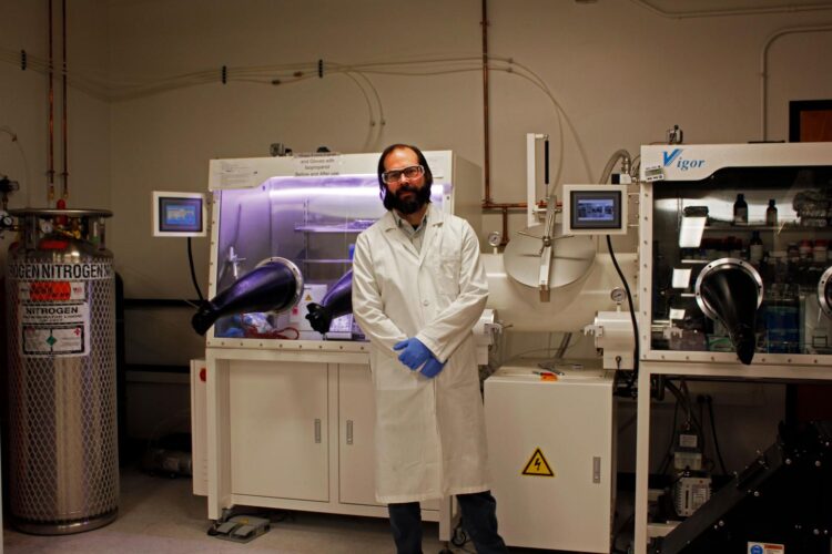
University of Arizona engineering professor harnesses the power of perovskites with a $700,000 grant from the Department of Energy Solar Energy Technologies Office.

Credit: University of Arizona College of Engineering
Imagine a television so thin that it could be rolled up like a newspaper, or a thin film that could coat an entire building and generate solar power. Perovskites could make this possible.
Perovskite is a type of mineral, but the word can also refer to a range of lab-made materials that share the same unique crystalline structure and exhibit properties like photoconductivity and the ability to be made into inks. The latter property is what enables perovskites to be printed out onto flexible pieces of plastic – similar to the way newspapers are printed. This could make it possible to someday print out highly efficient and ultra-thin solar cells, or something like a television or an LED light that is thin enough to be rolled up.
“To me, the potential flexibility and light weight of perovskites offers key competitive advantages in applications such as wearables, avionics, and disaster relief power where size and portability are critical constraints,” said Adam Printz, an assistant professor of chemical and environmental engineering at the University of Arizona. “Perhaps most exciting is that these benefits come without any significant tradeoff in device performance.”
The reason perovskites aren’t yet used more widely, is that, as a relatively new technology, they’re still very unstable. To overcome the instability, Printz has developed a new printing process called restricted area printing by ink drawing, or RAPID. He received a three-year, $700,000 grant from the Department of Energy Solar Energy Technologies Office (SETO) to advance the method.
Printz was selected as a part of the SETO Fiscal Year 2020 Perovskite Funding Program, which aims to rapidly increase affordable solar deployment, achieve the nation’s clean energy goals, and create high-paying U.S. jobs. His co-investigators are Erin Ratcliff, UArizona associate professor of chemical and environmental engineering; and Neal Armstrong, UArizona Regents Professor Emeritus of Chemistry and Biochemistry and Optical Sciences.
“This effort is an exciting opportunity for UArizona and the College of Engineering to lead in the area of processing printable solar materials, a key strategic area in the Institute for Energy Solutions and Arizona Institutes for Resilience,” Ratcliff said. “Metal halide perovskites are a very hot technology, and there is a lot of industry interest and excitement. It will be an excellent training opportunity for our students for years to come.”
Solar Power and the Spaces Between
Solar energy is one of the areas in which perovskites have the greatest potential. Since the 1950s, most solar cells have been made of silicon wafers, which convert light into electricity. Standard industrial silicon solar cells typically do this with about 18% to 22% efficiency. Perovskites are a much newer technology, but their efficiency is increasing at an unprecedented rate – from about 3% in 2006 to 25% today. Perovskite solar cells also cost less to produce than their silicon counterparts because they require far less material and production time.
Printz and his team started developing their perovskite printing process in late 2019, and they’ve been able to demonstrate on a small scale with 3D-printed parts how it works – using “whatever they had lying around in the lab.” This funding enables them to create a more reproducible and scalable version.
Perovskite materials are made by spreading a thin layer of specialized ink over a surface, then heating the ink to cause the formation of the perovskite crystalline structure. This printed film consists of many tiny grains separated by boundary areas. Under a high-powered microscope, it looks like dry, cracked mud. It’s in these boundary areas – which are more chemically reactive than the grains themselves – where things can get tricky.
“These boundary areas can actually interact with moisture in the air and cause the perovskite to convert into a completely different material that does not absorb light – which makes for a terrible solar cell,” Printz said. “We want to minimize grain boundary surface area so that those reactions don’t happen, and the perovskite is more likely to stay perovskite.”
Thus, the aim of RAPID is to produce as few boundary areas as possible. It does this by using a confined printing area so large grains can form without the solvent evaporating too quickly in the heat. Bigger grains mean reduced boundary area between grains, and reduced boundary area equates to more stability and efficiency.
Over the course of this three-year project, Printz and his team aim to reduce the grain boundaries by 90%. They also hope to improve the perovskite solar cells’ efficiency stability, or their ability to maintain efficiency over time, by 50%.
“When we get RAPID working at scale, we are hopeful that it will have profound impacts on the production of perovskites, significantly improving the stability of these low-cost and high efficiency devices,” Printz said.
###
Media Contact
Emily Dieckman
[email protected]
Original Source
https:/


