• HOME
  • NEWS
  • EXPLORE
    • CAREER
      • Companies
      • Jobs
    • EVENTS
    • iGEM
      • News
      • Team
    • PHOTOS
    • VIDEO
    • WIKI
  • BLOG
  • COMMUNITY
    • FACEBOOK
    • INSTAGRAM
    • TWITTER
Friday, May 15, 2026
BIOENGINEER.ORG
No Result
View All Result
  • Login
  • HOME
  • NEWS
  • EXPLORE
    • CAREER
      • Companies
      • Jobs
        • Lecturer
        • PhD Studentship
        • Postdoc
        • Research Assistant
    • EVENTS
    • iGEM
      • News
      • Team
    • PHOTOS
    • VIDEO
    • WIKI
  • BLOG
  • COMMUNITY
    • FACEBOOK
    • INSTAGRAM
    • TWITTER
No Result
View All Result
Bioengineer.org
No Result
View All Result
Home NEWS Science News Chemistry

Wider horizons for highly ordered nanohole arrays

Bioengineer by Bioengineer
March 13, 2021
in Chemistry
Reading Time: 3 mins read
0
IMAGE
Share on FacebookShare on TwitterShare on LinkedinShare on RedditShare on Telegram

More transition metals available to make ordered porous metallic oxide thin films

IMAGE

Credit: Tokyo Metropolitan University

Tokyo, Japan – Scientists from Tokyo Metropolitan University have developed a new method for making ordered arrays of nanoholes in metallic oxide thin films using a range of transition metals. The team used a template to pre-pattern metallic surfaces with an ordered array of dimples before applying electrochemistry to selectively grow an oxide layer with holes. The process makes a wider selection of ordered transition metal nanohole arrays available for new catalysis, filtration, and sensing applications.

A key challenge of nanotechnology is getting control over the structure of materials at the nanoscale. In the search for materials that are porous at this length scale, the field of electrochemistry offers a particularly elegant strategy: anodization using metallic electrodes, particularly aluminum and titanium, can be used to form ordered arrays of “nanoholes” in a metallic oxide layer. By getting the conditions right, these holes adopt highly ordered patterns, with tight control over their spacing and size. These ordered porous metallic oxide films are ideal for a wide range of industrial applications, such as filtration and efficient catalysis. But to get them out of the lab and into widespread use, production methods need to become more scalable and compatible with a wider range of materials.

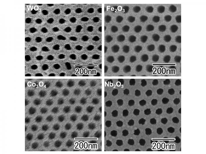
Enter a team led by Prof. Takashi Yanagishita of Tokyo Metropolitan University who have been pushing the boundaries of ordered nanohole array fabrication. In previous work, they developed a scalable method to make ordered nanohole arrays in aluminum oxide thin films. The team’s films could be made up to 70 mm in diameter, and easily detached from the substrates they are made on. Now, they have used these films to create similar patterns using a far wider range of transition metal oxides. By using the ordered nanoporous alumina as a mask, they used argon ion milling to etch ordered arrays of shallow dimples in the surfaces of various transition metals, including tungsten, iron, cobalt and niobium. Then by anodizing the dimpled surfaces, they found that thin metallic oxide layers formed with holes where the dimples were. Previous efforts had indeed made nanoscale holes in e.g. tungsten oxide films, but the holes were not ordered, with little control over their size or spacing, making this the first time ordered nanohole arrays have been made using these transition metal oxides. On top of that, by changing the properties of the mask, they directly demonstrated how they could easily tune the spacing between the holes, making their method applicable to a wide range of nanoporous patterns with different applications.

Exciting applications are waiting for these nanostructured films, including photocatalysis, sensing applications and solar cells. The team are confident that their new scalable, tunable method for making ordered nanohole arrays with freer choice of materials will help boost efforts to bring this exciting field of nanotechnology out of the lab, and into the wider world.

###

This work was supported by a JSPS KAKENHI Grant-in-Aid of Scientific Research, Grant Number JP20K05171.

Media Contact
Go Totsukawa
[email protected]

Related Journal Article

http://dx.doi.org/10.1016/j.elecom.2020.106916

Tags: Chemistry/Physics/Materials SciencesIndustrial Engineering/ChemistryMaterialsNanotechnology/MicromachinesOpticsTechnology/Engineering/Computer Science
Share12Tweet8Share2ShareShareShare2

Related Posts

Hanyang University Researchers Pinpoint 2.5 Nanometers as Minimum Coating Thickness for Durable Solid-State EV Batteries — Chemistry

Hanyang University Researchers Pinpoint 2.5 Nanometers as Minimum Coating Thickness for Durable Solid-State EV Batteries

May 15, 2026
Smart Hydrogels Revolutionize Information Security with Photo-Patterning and Multi-Stimuli Responsive Structural Colors — Chemistry

Smart Hydrogels Revolutionize Information Security with Photo-Patterning and Multi-Stimuli Responsive Structural Colors

May 15, 2026

Scientists Overcome Longstanding Challenge in Measuring Semiconductor Defects

May 14, 2026

Wall Design Highlights Deaf and Hard-of-Hearing Experience at #ASA190

May 14, 2026
Please login to join discussion

POPULAR NEWS

  • Research Indicates Potential Connection Between Prenatal Medication Exposure and Elevated Autism Risk

    843 shares
    Share 337 Tweet 211
  • New Study Reveals Plants Can Detect the Sound of Rain

    729 shares
    Share 291 Tweet 182
  • Salmonella Haem Blocks Macrophages, Boosts Infection

    62 shares
    Share 25 Tweet 16
  • Breastmilk Balances E. coli and Beneficial Bacteria in Infant Gut Microbiomes

    58 shares
    Share 23 Tweet 15

About

We bring you the latest biotechnology news from best research centers and universities around the world. Check our website.

Follow us

Recent News

Hanyang University Researchers Pinpoint 2.5 Nanometers as Minimum Coating Thickness for Durable Solid-State EV Batteries

Axonic Spine Synapses Trigger Action Potentials, Direct Signals

New Study Uncovers Why Breast Cancer Becomes More Lethal with Age

Subscribe to Blog via Email

Enter your email address to subscribe to this blog and receive notifications of new posts by email.

Join 82 other subscribers
  • Contact Us

Bioengineer.org © Copyright 2023 All Rights Reserved.

Welcome Back!

Login to your account below

Forgotten Password?

Retrieve your password

Please enter your username or email address to reset your password.

Log In
No Result
View All Result
  • Homepages
    • Home Page 1
    • Home Page 2
  • News
  • National
  • Business
  • Health
  • Lifestyle
  • Science

Bioengineer.org © Copyright 2023 All Rights Reserved.