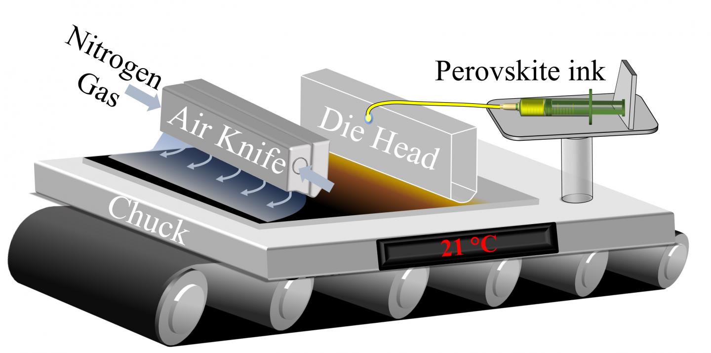
Credit: HZB/Jinzhao Li
They have improved a process for vertically depositing a solution made from an inexpensive perovskite solute onto a moving substrate below. Not only have they discovered the crucial role played by one of the solvents used, but they have also taken a closer look at the aging and storage properties of the solution.
Solar cells made of crystalline silicon still account for the lion’s share of roof installations and solar farms. But other technologies have long since become established as well – such as those that convert sunlight into electrical energy through use of extremely thin layers of solar-cell material deposited upon a substrate. The perovskite solar cells that Prof. Eva Unger and her team at the Helmholtz-Zentrum Berlin (HZB) are researching belong to this group. “These are the best solar cells to date that can be made using a 2D ink”, the researcher explains. “And now their efficiencies are approaching those for cells made of crystalline silicon.”
*Developing scalable methods*
Many methods have been developed and used to fabricate small test cells in the laboratory, where they can be studied and improved. But industrial-scale fabrication is still a long way off. Unger knows from her own experience: “Unfortunately, processes that are optimised for fabricating small surface areas cannot always be scaled up.” In other words: Not everything that works perfectly in the lab also necessarily works economically on the factory floor. “That’s why we are taking the next step and developing scalable methods. This means our team is focussing on processes for coating larger surfaces.” At the Hybrid Silicon Perovskite Research, Integration & Novel Technologies (HySPRINT) Innovation Lab, an infrastructure for collaboration between HZB and industry, the team is concentrating on processes that have already proven their importance in industry to start with.
“We have experimented here with slot-die coating”, she explains. In this process, the “ink”, as the thin liquid solution of perovskite precursor, solvent, and additive is known in the trade, flows from a slit-shaped nozzle and falls like a curtain onto the glass substrate being conveyed below that will later become a solar cell. After application, crystallisation begins. An ultra-thin layer of a semiconducting perovskite structure grows that gives the material group its name and the solar cell its capabilities. Unger, together with her team members doctoral student Jinzhao Li and Dr. Janardan Dagar, have now discovered that the exact amount of an organic solvent called dimethyl sulfoxide (DMSO) in the material ink is critical for this process. Unger uses it as an additive because it has an amazing effect on the ink. “DMSO induces crystallisation nuclei for the perovskite”, says the researcher. Crystallisation nuclei usually are tiny grains that help jump-start a crystal and promote its growth. “During X-ray diffraction experiments at BESSY II, we saw quite a big difference between inks with and without DMSO added”, the physical chemist explains.
*It’s the amount that counts*
However, as her team has found out in many experiments, the amount added plays a decisive role here. More DMSO favours crystal growth – up to a certain point. If this is exceeded, other processes come into play and the resulting microstructure reduces the performance of the solar cells. “It’s like seasoning a soup”, says Unger. “If you add too little, it remains bland. If you add too much, it won’t taste good either. So you need to add just the right amount to make it best.” In addition to the optimal composition, the HZB team has also thoroughly investigated the ageing processes and thus the storage life of the inks. “This is an aspect that has received little attention so far”, Unger explains. “The age of a perovskite precursor ink can influence device performance. This is an important factor that must be considered when developing inks and processes.”
###
Media Contact
Dr. Eva Unger
[email protected]
Original Source
https:/
Related Journal Article
http://dx.


